Method of Fabricating Semiconductor Device Isolation Structure

a technology of isolation structure and semiconductor device, which is applied in the direction of semiconductor devices, electrical equipment, transistors, etc., can solve the problems of affecting the performance of the device, affecting the manufacturing process, and affecting the production efficiency of small appliances, so as to achieve reliable isolation structure, increase manufacturing costs, and high aspect ratio

Active Publication Date: 2008-12-11
TAIWAN SEMICON MFG CO LTD
View PDF5 Cites 6 Cited by
  • Summary
  • Abstract
  • Description
  • Claims
  • Application Information

AI Technical Summary

Benefits of technology

[0018]An advantage of a preferred embodiment of the present invention is that a reliable isolation structure may be formed in a semiconductor substrate even having very small dimension and a high aspect ratio. Produced with a reentrant profile, it may even prove superior to prior shallow-trench isolation structures.
[001

Problems solved by technology

This effort results not only in greater challenges during the fabrication process itself, but gives rise to certain electrical problems, such as current leakage, that detrimentally effect of the performance of the device.
As mentioned above, however, there is strong market pressure to produce smaller appliances, which in turn require even smaller chips.
The devices on these chips are often being reduced in size, a phenomenon sometimes

Method used


Image

  • Method of Fabricating Semiconductor Device Isolation Structure
  • Method of Fabricating Semiconductor Device Isolation Structure
  • Method of Fabricating Semiconductor Device Isolation Structure

Examples


Embodiment Construction

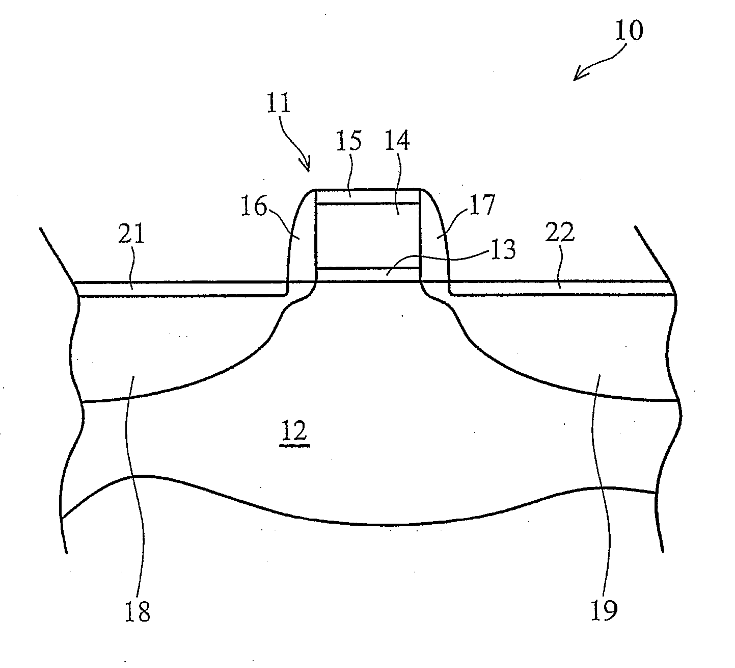
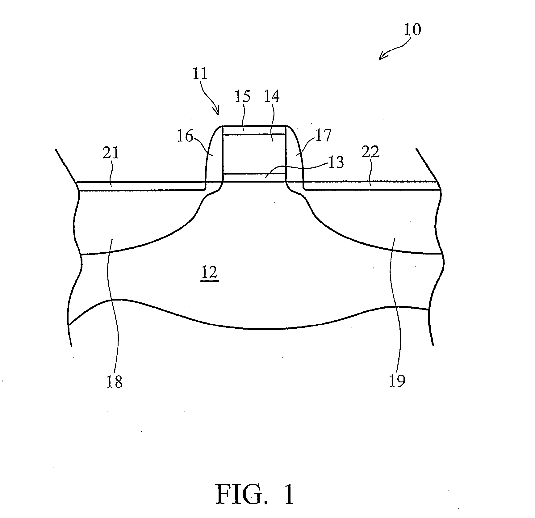
[0029]The making and using of the presently preferred embodiments are discussed in detail below. It should be appreciated, however, that the present invention provides many applicable inventive concepts that can be embodied in a wide variety of specific contexts. The specific embodiments discussed are merely illustrative of specific ways to make and use the invention, and do not limit the scope of the invention. The present invention will be described with respect to preferred embodiments in a specific context, namely the formation of a single isolation structure in a semiconductor substrate. The invention may also be applied, however, in other applications as well. The embodiments described below, in other words, are intended to be illustrative rather than limiting. For example, a great many isolation structures are normally created simultaneously at selected sites across a semiconductor wafer.

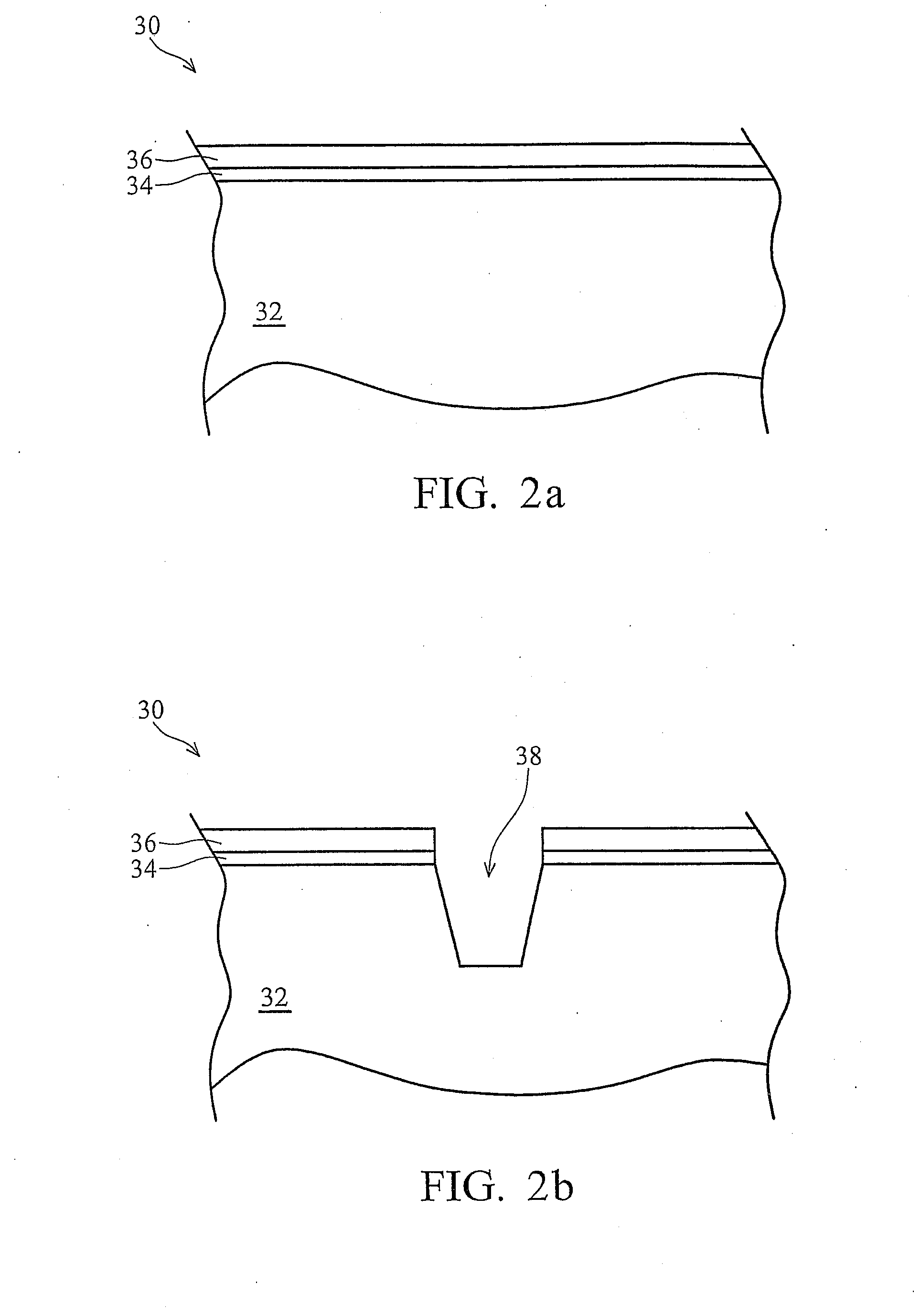
[0030]As mentioned above, isolation structures are used in semiconductor devices to isola...


PUM


Abstract

A semiconductor device including reentrant isolation structures and a method for making such a device. A preferred embodiment comprises a substrate of semiconductor material forming at least one isolation structure having a reentrant profile and isolating one or more adjacent operational components. The reentrant profile of the at least one isolation structure is formed of substrate material and is created by ion implantation, preferably using oxygen ions applied at a number of different angles and energy levels. In another embodiment the present invention is a method of forming an isolation structure for a semiconductor device performing at least one oxygen ion implantation.

Description

TECHNICAL FIELD[0001]The present invention relates generally to the fabrication of semiconductor devices, and more particularly relates to a semiconductor device isolation structure and a method for fabricating such a structure using ion implantation.BACKGROUND[0002]Semiconductor devices are very small electronic components that may be used to form integrated circuits, the basic operational portions of the now-familiar electronics products called chips. A chip is, generally speaking, a semiconductor die that has been encapsulated in a hard plastic or similar enclosure. Sometimes a number of interconnected dice are housed in the same enclosure. Before encapsulation, leads, traces, or other conductive devices external to the die itself are added to provide electrical connections between integrated circuits on the die and other electronic devices external to the chip. The chips are then often mounted onto printed wire boards and installed in such appliances such as personal computers, ...

Claims


Application Information

Patent Timeline
IPC IPC(8): H01L29/94
CPCH01L21/26506H01L21/26586H01L29/6659H01L29/7833H01L21/324H01L21/762H01L21/823481H01L21/26533H01L21/266H01L21/76202H01L29/0649
Inventor YU, CHEN-HUAYEH, CHEN-NANFU, CHU-YUNCHEN, DING-YUAN
Owner TAIWAN SEMICON MFG CO LTD
Why Eureka
Try Eureka