

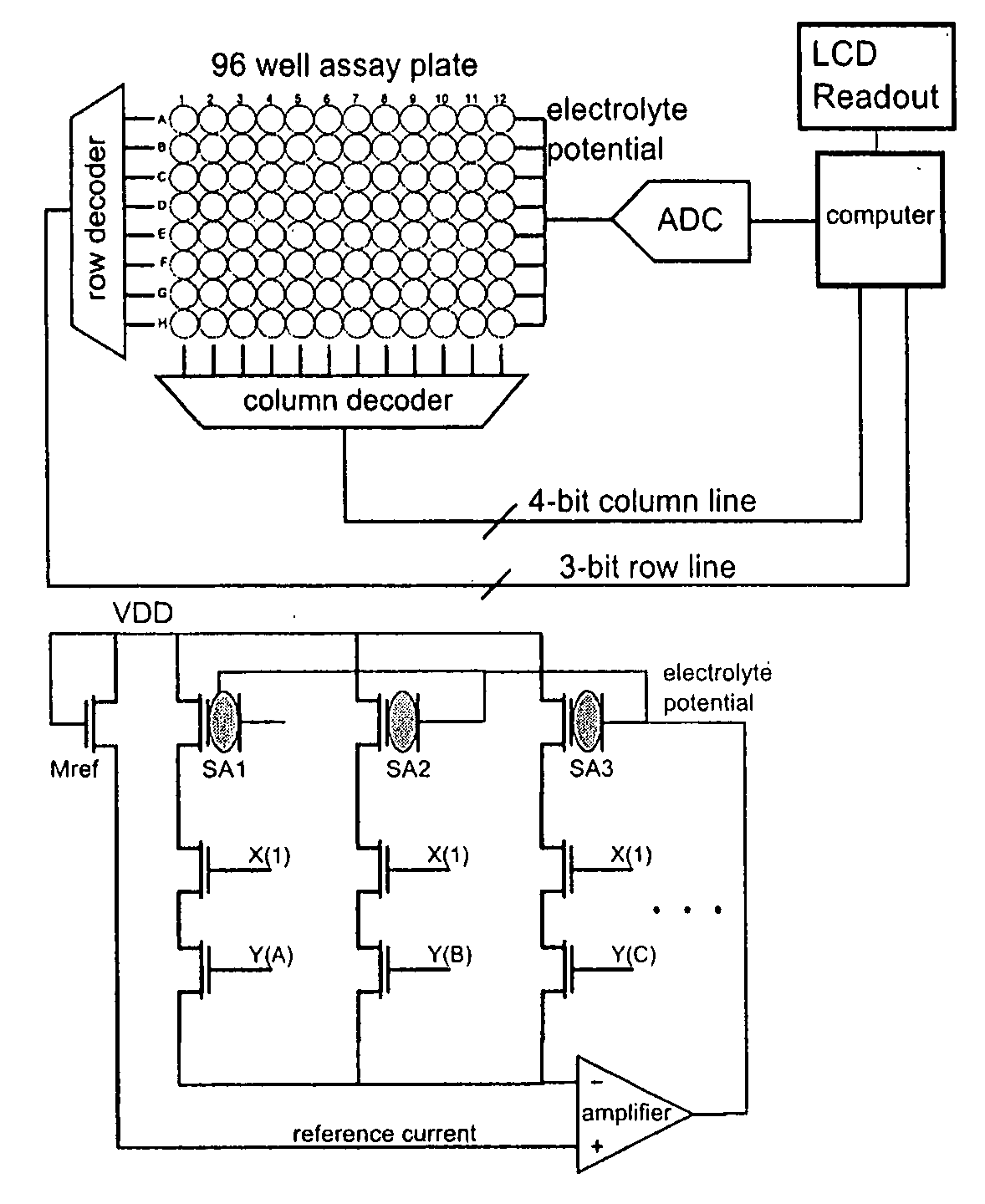
Apparatus for microarray binding sensors having biological probe materials using carbon nanotube transistors
a technology of carbon nanotube transistors and microarrays, applied in thermoelectric device junction materials, diaphragms, immobilised enzymes, etc., can solve the problems of large amount of reagents, complex protocols, laborious techniques, etc., and achieve low ionic buffer, rapid hybridization, and limited sensitivity
- Summary
- Abstract
- Description
- Claims
- Application Information
AI Technical Summary
Benefits of technology
Problems solved by technology
Method used
Image

Examples
example 1
Use of Catalysts in Forming CNTs
[0221] At least two methods may be employed for creating Fe nanoparticles that act as catalysts for CNT growth: a). Ultra high vacuum deposition of Fe at a thickness of less than 0.5 nanometers; and b). Formation of FePt particles using “nanocluster gun” technique of Ping Wang at Univ. of Minnesota. FIGS. 24 and 25 show the growth of CNT for each catalyst. Both produce CNTs, but longer and sparsely distributed CNT's are formed on FePT clusters. Any conventional method for forming CNTs may then be used with the Fe-containing catalysts.
example 2
Gold Deposition to Connect NT Channel to S and D Electrodes
[0222] Gold contracts are made using standards contact photolithography techniques and depositing gold to the defined area using physical vapor deposition technique. Briefly, standard contact photolithography involves coating the substrate / sample with a light-sensitive material, or a photoresist, which dissolves or hardens depending on the type upon exposure to light and subsequent developer solution. Patterns from a pre-drawn mask are transferred to the photoresist by exposing it to an ultraviolet light through the mask. A physical vapor deposition technique involves vaporizing solid material of interest, which is gold for this particular purpose, through various methods such as: resistive heating, electron beam heating, plasma sputtering, such that the vapor condenses on the substrate / sample thereby creating a thin film on the substrate / sample. Gold adhesion towards the oxide substrate / sample is improved by first depositi...
example 3
Preparation of Aluminum Oxide Gate Material
[0223] A preferred method for creating oxides, such as aluminum or hafnium oxides is by atomic layer deposition. Atomic layer deposition (ALD) is a known deposition method in which a film is built up one atomic layer at a time by saturating the functional group of the surface with a suitable precursor. The ALD cycle / steps to deposit aluminum oxide starts by saturating the surface, which inevitably contains hydroxyl group due to air moisture, with trimethyl aluminum (TMA). After excess / unreacted trimethyl aluminum is removed, water vapor is introduced to convert the methyl group of TMA to hydroxyl group, releasing methane as the byproduct. The newly converted hydroxyl group is now ready to react with another cycle of TMA exposure. Cycles of introduction of TMA and water vapor are repeated until the desired thickness is achieved.
PUM
| Property | Measurement | Unit |
|---|---|---|
| separation distance | aaaaa | aaaaa |
| thick | aaaaa | aaaaa |
| temperature | aaaaa | aaaaa |
Abstract
Description
Claims
Application Information