Probe pins zero-point detecting method, and prober

a probe pin and zero-point detection technology, applied in semiconductor/solid-state device testing/measurement, fault location by increasing destruction at fault, etc., can solve the problem of difficulty in bringing wafer w and probe pins b>8/b>a into contact at high accuracy, needle pressure for testing may damage the electrode pad and its underlying layer, and gold wafer cannot meet such a demand for a lower needle pressur

Inactive Publication Date: 2006-04-04
OCTEC INC +1
View PDF7 Cites 110 Cited by
  • Summary
  • Abstract
  • Description
  • Claims
  • Application Information

AI Technical Summary

Benefits of technology

[0014]The present invention solves at least one of the above problems. The present invention provides probe pins zero-point detecting method which can detect the zero point of probe pins with high accuracy, and preferably which can reliably prevent any damage to the device caused by the needle pressure during testing, and a prober which can detect the zero point.

Problems solved by technology

It is, however, difficult to bring the wafer W and probe pins 8A into contact with each other at high accuracy.
Particularly, as the thickness of the wiring layer or the like of the device decreases and the number of layers in the multilayered wiring layer increases these days, the needle pressure for testing may damage the electrode pad and its underlying layer.
A gold wafer cannot meet such a demand for a lower needle pressure.

Method used


Image

  • Probe pins zero-point detecting method, and prober
  • Probe pins zero-point detecting method, and prober
  • Probe pins zero-point detecting method, and prober

Examples


first embodiment

[0048]The characteristic features of the present invention will now be mainly described on the basis of the first embodiment shown in FIGS. 1A to 5B by denoting the same or corresponding portions as in the prior art with the same reference numerals.

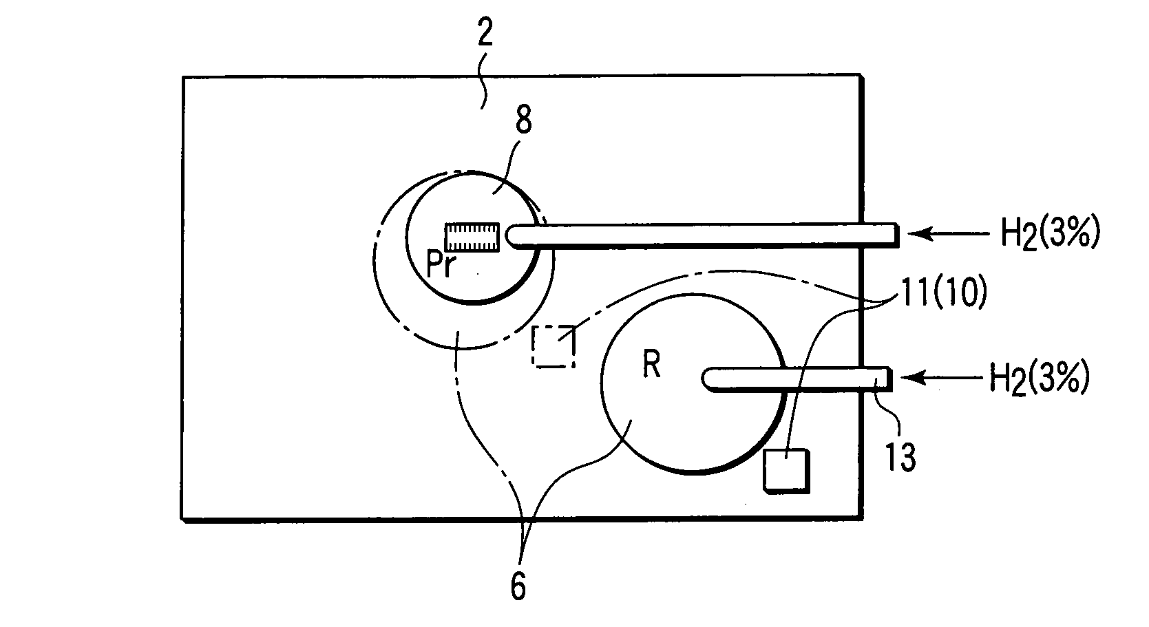
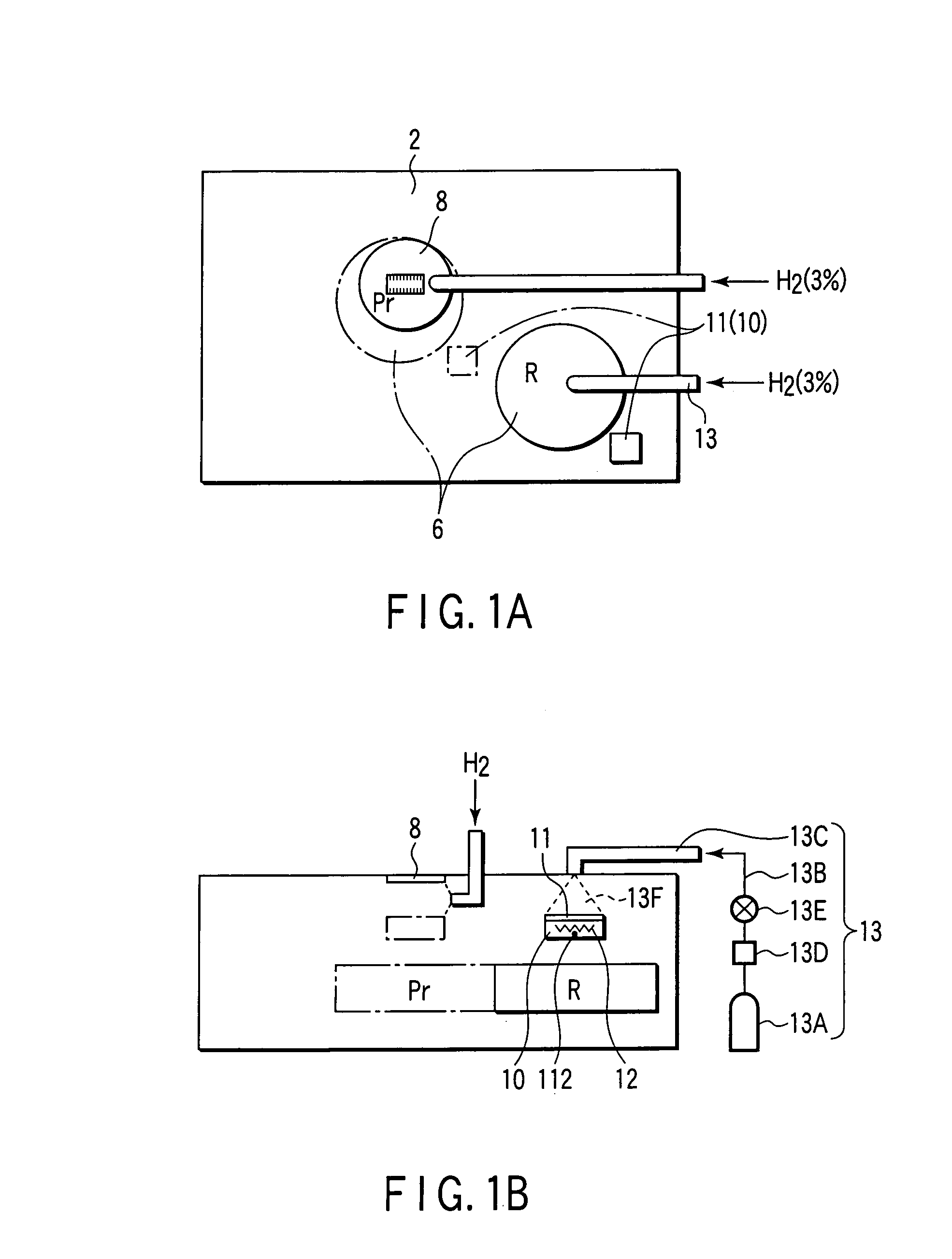
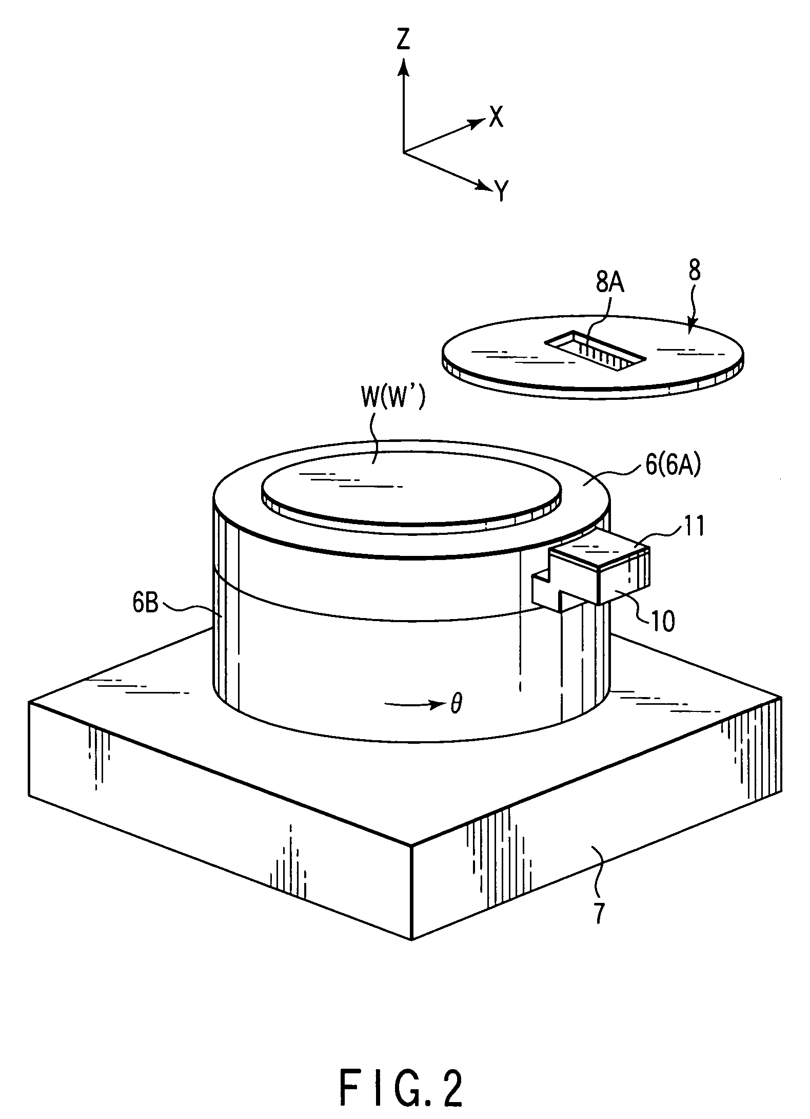
[0049]A prober of this embodiment is formed in the same manner as that of a conventional prober except that it has a zero-point detection plate 11 and a reducing mechanism (12, 13) in a prober chamber 2 as shown in, e.g., FIGS. 1A, 1B, and 2. More specifically, the prober chamber 2 has a stage 6 which places a wafer W thereon and moves in the horizontal and vertical directions, a moving mechanism 7 and rotary mechanism 6B which move the stage 6 in the X, Y, and Z directions and in a θ direction, respectively, and a probe card 8 which is arranged above the stage 6 and has a plurality of probe pins 8A. In the prober chamber 2, the probe pins 8A are brought into contact with electrodes P (FIG. 5A) of an object W′ to be tested (e.g., device) ...

second embodiment

[0063]the present invention will be described. According to this embodiment, as shown in FIGS. 4A and 4B, a copper wafer having a surface made of copper can be used as a zero-point detection plate 11A. The zero-point detection plate 11A can be stored in a storing portion 1A (FIG. 8A) in a loader chamber 1. When a stage 6 has a heating mechanism for high-temperature testing of a wafer W, the heating mechanism can be used as a heating mechanism for reducing the copper wafer. As a gas supply mechanism 13, a type which is arranged in a prober chamber 2 in the same manner as in the above embodiment can be used.

[0064]A zero point detecting method according to the second embodiment will be described. The zero-point detection plate 11A is extracted from the loader chamber and placed on the stage 6 in the prober chamber. The zero-point detection plate 11A may be heated by an electroresistive heating mechanism 12A of the stage 6 to a temperature that can reduce copper oxide. The stage 6 moves...

fourth embodiment

[0068]The fourth embodiment will be described. According to this embodiment, a storing portion 1A which stores a zero-point detection plate is arranged in a loader chamber, as shown in FIG. 8A. As a zero-point detection plate 11A, the copper wafer shown in FIG. 4A can be employed.

[0069]As shown in FIG. 8B, an electroresistive heating mechanism 12A to heat the zero-point detection plate 11A can be arranged in the loader chamber (e.g., in a storing portion 1A). Similarly, the heating mechanism can be a lamp 12B, as shown in FIG. BC.

[0070]A reducing gas supply mechanism 13 can be arranged in the storing portion 1A.

[0071]When the heating mechanism and reducing gas supply mechanism are to be arranged in the storing portion 1A, the copper wafer is heated and blown with a reducing gas in the storing portion 1A, as shown in FIG. 8A, so that the copper oxide surface on the copper wafer is reduced to form reduced copper. The copper wafer in this state is transported from a loader chamber 1 to...


PUM


Abstract

A zero-point detecting method of this invention is performed prior to testing the electrical characteristics of a wafer by bringing an object to be tested on a stage and probes of a probe card into contact with each other. The surface of a zero-point detection plate is made of a conductive material (e.g., copper). The zero-point detection plate is used to detect a zero point as a position where the surface of the object to be tested comes into contact with the probe pins.

Description

CROSS REFERENCE TO RELATED APPLICATIONS[0001]This is a Continuation Application of PCT Application No. PCT / JP2004 / 001534, filed Feb. 13, 2004, which was published under PCT Article 21(2) in Japanese.[0002]This application is based upon and claims the benefit of priority from prior Japanese Patent Application No. 2003-042285, filed Feb. 20, 2003, the entire contents of which are incorporated herein by reference.BACKGROUND OF THE INVENTION[0003]1. Field of the Invention[0004]The present invention relates to a method of detecting the zero point of probe pins accurately, and a prober. Preferably, the present invention relates to probe pins zero-point detecting method which can largely reduce the needle pressure between probe pins and an object to be tested during testing, and a prober which can detect the zero point.[0005]2. Description of the Related Art[0006]In the process of manufacturing a semiconductor device, a prober is used to test the electrical characteristics of devices forme...

Claims


Application Information

Patent Timeline
Patent Type & Authority Patents(United States)
IPC IPC(8): G01R31/02G01R1/06G01R1/067G01R31/28H01L21/66
CPCG01R1/06794G01R31/2891G01R31/2887H01L22/00
Inventor OKUMURA, KATSUYAFURUYA, KUNIHIRO
Owner OCTEC INC
Why Eureka
Try Eureka