Semiconductor device with electrically coupled spiral inductors

a spiral inductors and electromagnetic technology, applied in the direction of inductances, basic electric elements, inductance/transformers/magnets, etc., can solve the problems of low coupling coefficient, k, and quality factor, q, of such a coupled pair of inductors

Inactive Publication Date: 2006-04-04
MICRON TECH INC
View PDF24 Cites 14 Cited by
  • Summary
  • Abstract
  • Description
  • Claims
  • Application Information

AI Technical Summary

Problems solved by technology

However, the coupling coefficient, k, and the quality factor, Q, of such a coupled pair of inductors has been relatively low, and multiple coupled pairs have been required to perform the aforementioned additions and subtractions.

Method used


Image

  • Semiconductor device with electrically coupled spiral inductors
  • Semiconductor device with electrically coupled spiral inductors
  • Semiconductor device with electrically coupled spiral inductors

Examples


Embodiment Construction

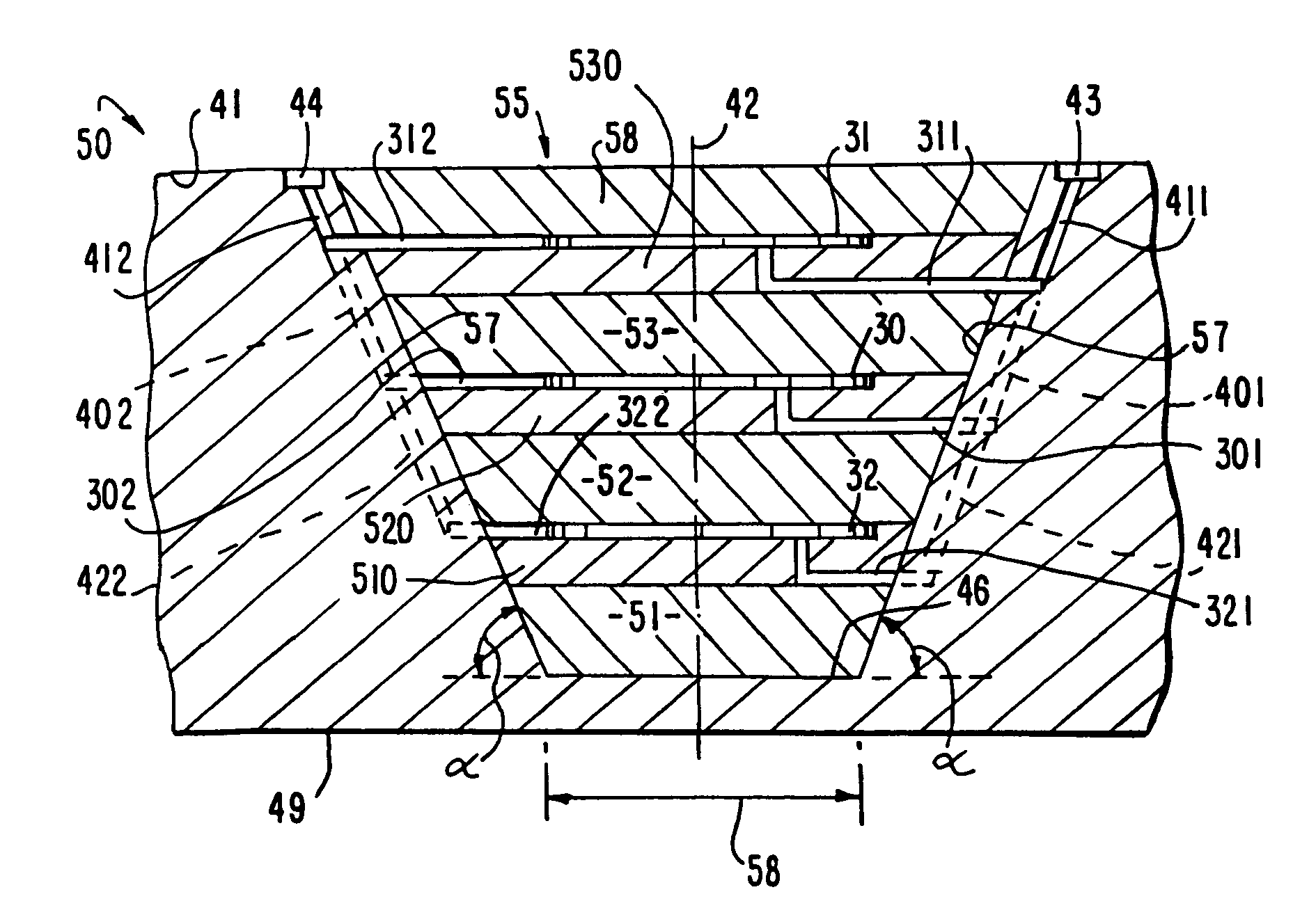
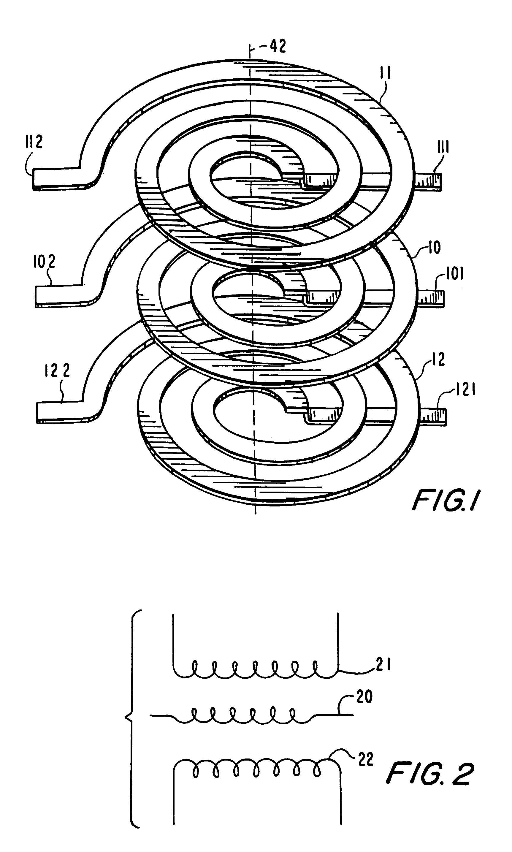
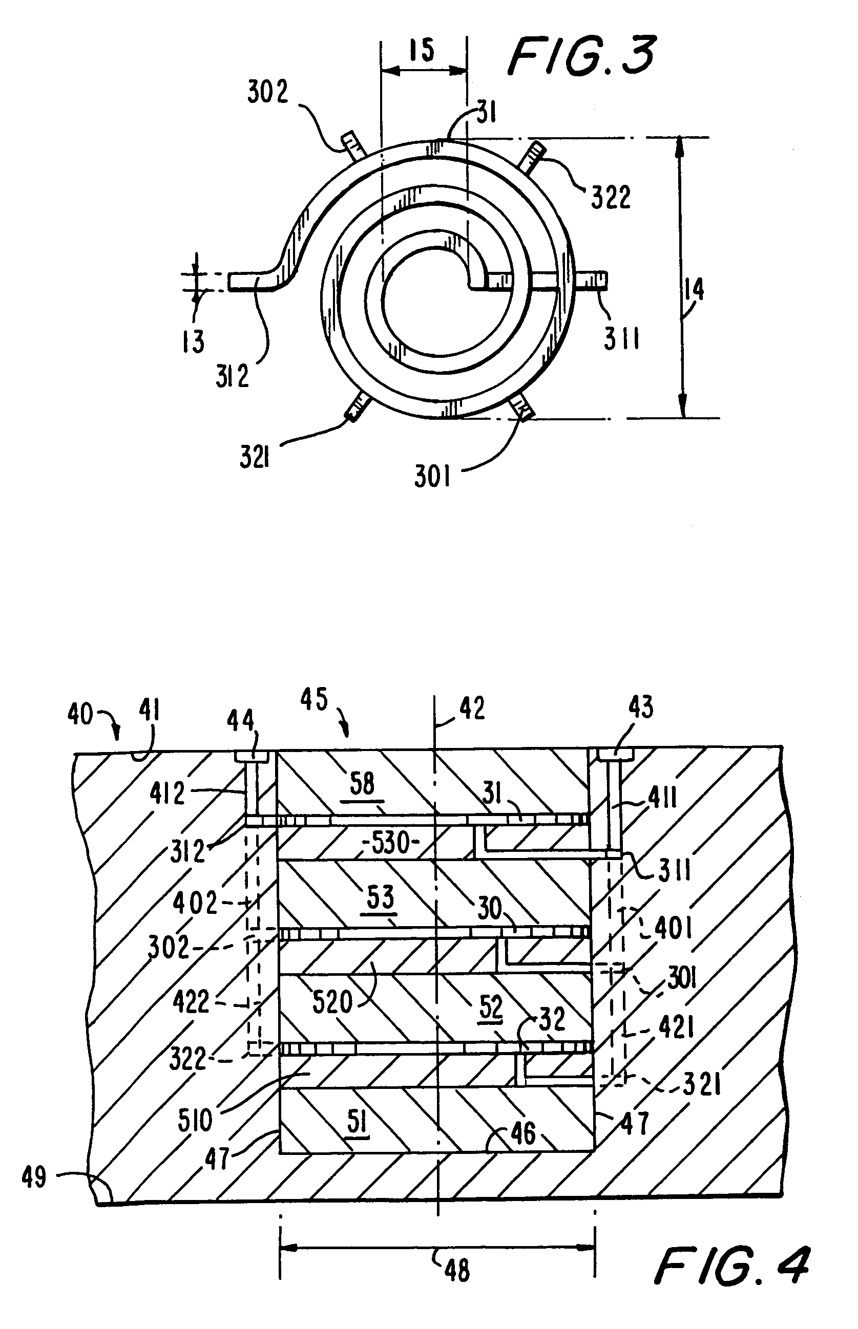
[0014]At this point, it useful to note that the time-varying voltage induced in an inductor having inductance L2 by a time-varying current i1(t) flowing in another inductor to which it is coupled, the other inductor having inductance L1, is V2(t)=m(di1 / dt), where m=k(L1L2)0.5, k being the coupling coefficient.

[0015]For example, it is well known that the time-varying voltage in inductor L1 is V1(t)=L1(di1 / dt). Therefore, (di1 / dt)=V1(t) / L1. It follows that:

[0016]V2⁡(t)=mV1⁡(t) / L1⁢⁢=(k⁡(L1⁢L2)0.5 / L1)⁢V1⁡(t)⁢⁢=V1⁡(t)⁢k⁡(L2 / L1)0.5.

[0017]For an ideal transformer, where k=1:

V2(t)=V1(t) (L2 / L1)0.5, or

V2(t) / V1(t)=(L2 / L1)0.5.

[0018]Because Ln∝Nn2, V2(t) / V1(t)∝(N2 / N1), which is the familiar relation for an ideal transformer. However, the actual induced voltage V2(t) in the second inductor is a function not of the voltage V1(t) applied to the first inductor, but of the current i1(t) flowing in the first inductor, and of the coupling coefficient, k, as set forth above.

[0019]As described above, in...


PUM

PropertyMeasurementUnit
angleaaaaaaaaaa
diameteraaaaaaaaaa
depthaaaaaaaaaa

Abstract

Multiple coupled inductors are formed in a well in a semiconductor device. The inductors, which preferably are spiral inductors, are strongly coupled with high quality factors. The coupled inductors may be used as efficient signal splitting and combining circuits.

Description

[0001]This is a continuation of commonly-assigned U.S. patent application Ser. No. 10 / 008,900, filed Dec. 5, 2001, now U.S. Pat. No. 6,635,948.BACKGROUND OF THE INVENTION[0002]This invention relates to an integrated circuit structure having a plurality of inductors arranged so that different pairs of inductors are electrically coupled to one another. More particularly, this invention relates to an integrated circuit structure in which at least three inductors are fabricated adjacent one another in a well in the structure. This invention also relates to power splitters and combiners using such coupled inductors.[0003]It is known that inductors can be formed on the surface of a semiconductor substrate, and that one individual inductor can be coupled to another individual inductor. It is also known that such a coupled pair of inductors can be used as a transformer in, among other things, an RF circuit in which signals must be added or subtracted to perform signal processing and / or modu...

Claims


Application Information

Patent Timeline
Patent Type & Authority Patents(United States)
IPC IPC(8): H01F5/00H01F17/00H01F41/04H01L21/02H01L23/522H01L27/08
CPCH01L23/5227H01L27/08H01L28/10H01F17/0013H01F41/041H01L2924/0002H01L2924/00
Inventor AHN, KIE Y.FORBES, LEONARD
Owner MICRON TECH INC
Why Eureka
Try Eureka