Via/line inductor on semiconductor material

a technology of inductor and semiconductor material, which is applied in the field of integrated circuits, can solve the problems of degrading the inductor performance of cmos technology, achieving high-performance on-chip inductors, and still remains a major problem, and achieves the effect of increasing the surface area of spiral inductors and increasing the high quality factor (q)

Inactive Publication Date: 2006-07-18
CHARTERED SEMICONDUCTOR MANUFACTURING
View PDF8 Cites 31 Cited by
  • Summary
  • Abstract
  • Description
  • Claims
  • Application Information

AI Technical Summary

Benefits of technology

[0013]The present invention provides a spiral inductor including a substrate and an inductor dielectric layer over the substrate having a spiral opening provided therein. A spiral inductor is in the spiral opening with the inductor including a plurality of parallel spir...

Problems solved by technology

However, despite efforts by many researchers having skill in the art, achieving high performance on-chip inductors, i.e., high quality factor (Q), still remains a major problem especially when radio frequency integrated circuits (RFICs) are built on silicon.
In addition, high dynamic resistance of metal lines at GHz frequency ranges further degrades the inductor performance in CMOS technology as compared to those fabricated in monolithic microwave integrated circuits (MMICs).
Despite achieving good results, industries are reluctant to adopt such a technique because of reliability issues such as packaging yield, as well as long-term mechanical stability.
The most critical factor hinde...

Method used


Image

  • Via/line inductor on semiconductor material
  • Via/line inductor on semiconductor material
  • Via/line inductor on semiconductor material

Examples


Embodiment Construction

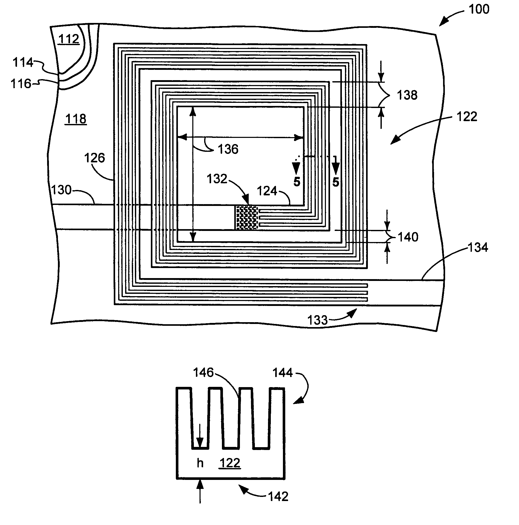
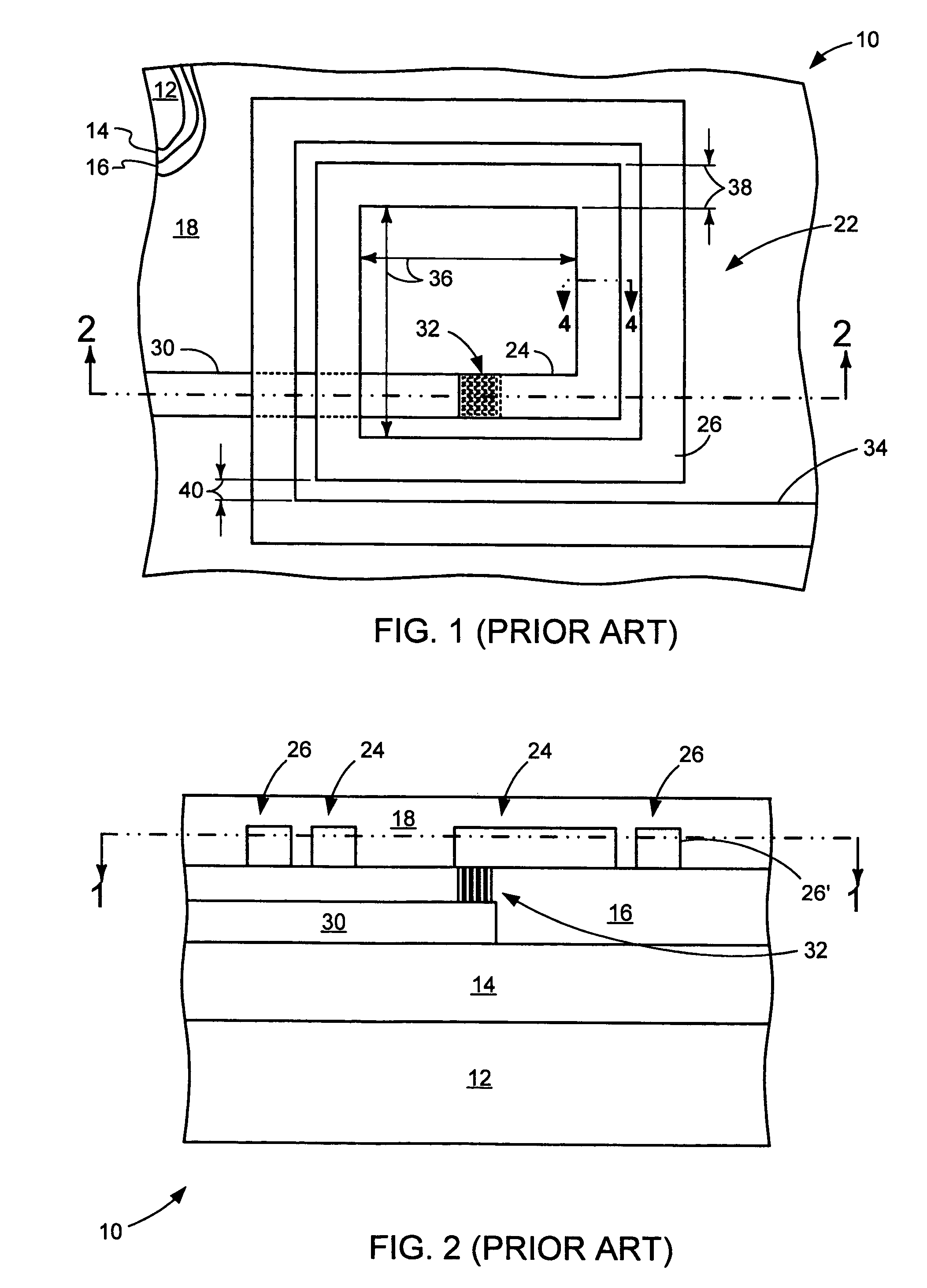
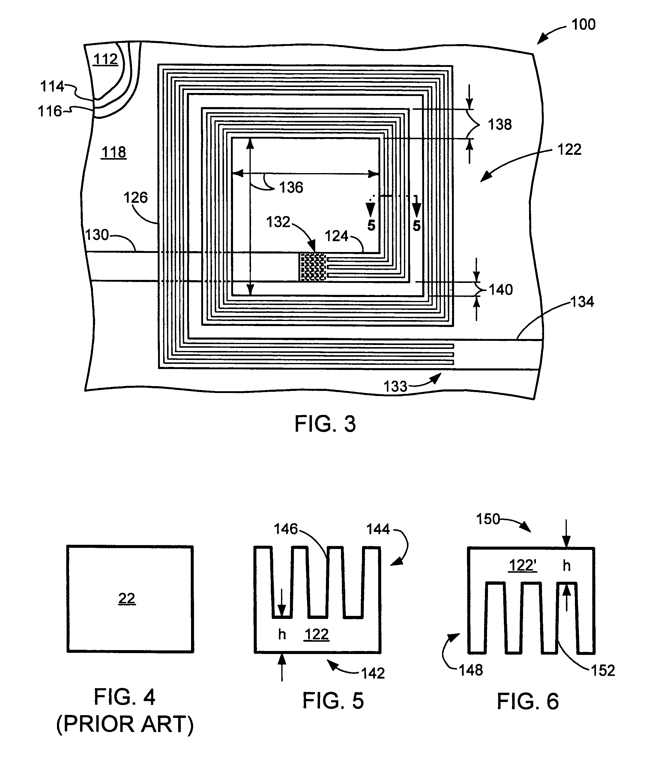
[0021]Referring now to FIG. 1 (PRIOR ART), therein is shown a cross-sectional view of a prior art on-chip inductor 10 along line 1—1 of FIG. 2 (PRIOR ART). A substrate 12, of a material such as silicon, has a plurality of dielectric layers formed thereon of a material such as silicon dioxide. Sequentially, a field dielectric layer 14 (such as a field oxide), a connecting interlayer dielectric (ILD) layer 16 (such as a silicon oxide), and an inductor ILD layer 18 are formed over the substrate 12. Embedded within the inductor ILD layer 18 is a prior art spiral inductor 22.

[0022]The term “over” as used in herein is defined vertically above a horizontal plane parallel to the conventional surface of a wafer on which the on-chip inductor is formed regardless of the orientation of the wafer. Terms, such as “on”, “below”, “higher”, “lower”, “above”, and “under”, are defined with respect to the horizontal plane.

[0023]The term “processed” or “forming” as used herein to refer to the formation ...


PUM

PropertyMeasurementUnit
Semiconductor propertiesaaaaaaaaaa

Abstract

A spiral inductor is provided including a substrate and an inductor dielectric layer over the substrate having a spiral opening provided therein. The spiral inductor is in the spiral opening with the spiral inductor including a plurality of parallel spiral vias connected together at center proximate and center distal ends of the spiral inductor.

Description

CROSS-REFERENCE TO RELATED APPLICATION(S)[0001]This is a divisional of application Ser. No. 10 / 040,765, now U.S. Pat. No. 6,750,750 filed Dec. 28, 2001, which is hereby incorporated by reference herein.TECHNICAL FIELD[0002]The present invention relates generally to integrated circuits and more particularly to on-chip silicon-based inductors.BACKGROUND OF THE INVENTION[0003]Increasing demands for personal mobile communications equipment have motivated recent research activities to focus on the development of inexpensive, small size, low power consumption, and low noise level systems. To satisfy these requirements, one of the most important and indispensable circuit components is the on-chip silicon-based inductor.[0004]As a result, miniaturization of the inductor on silicon has become a current key research area and extensive work has been done in this area. However, despite efforts by many researchers having skill in the art, achieving high performance on-chip inductors, i.e., high ...

Claims


Application Information

Patent Timeline
IPC IPC(8): H01F5/00H01L21/02H01L21/822H01L27/04H01L27/08
CPCH01L27/08H01L28/10Y10T29/4902H01L27/04
Inventor ZHANG, JIONGWANG, YI MINCHU, SHAO-FU SANFORD
Owner CHARTERED SEMICONDUCTOR MANUFACTURING
Why Eureka
Try Eureka