Spiral inductor

a spiral inductor and inductor technology, applied in the direction of transformer/inductance details, transformer/inductance coil/winding/connection, etc., can solve the problems of high parasitic capacitance between metal lines, impede the operation of any circuit, increase the resistance of the inductor, etc., to reduce parasitic capacitance, improve the quality of the inductor, and reduce the loss

Inactive Publication Date: 2009-02-03
DSS TECH MANAGEMENT
View PDF6 Cites 31 Cited by
  • Summary
  • Abstract
  • Description
  • Claims
  • Application Information

AI Technical Summary

Benefits of technology

[0007]The present invention has been proposed in order to solve the problems in the related art described above. It is an object of the present invention to provide a spiral inductor capable of reducing parasitic capacitance between the metal lines of the inductor, reducing the loss due to eddy current or displaced current, and improving the quality of the inductor.

Problems solved by technology

One difficulty in forming the spiral structure using a series of straight lines, however, is that polarization occurs at the edges of the metal wire, causing increased resistance in the inductor and a high parasitic capacitance between the metal lines.
In particular, in configurations where the metal wire is formed directly on the semiconductor substrate, an eddy current may be generated on the semiconductor substrate, which impedes the operation of the any circuit, such as a transistor, which has been previously formed on the semiconductor substrate.
Thus, one difficulty is that it is difficult to produce a high-quality inductor on the semiconductor substrate due to the loss caused by eddy currents or displace currents generated by the inductor of the current art.

Method used


Image

  • Spiral inductor
  • Spiral inductor
  • Spiral inductor

Examples


embodiment 1

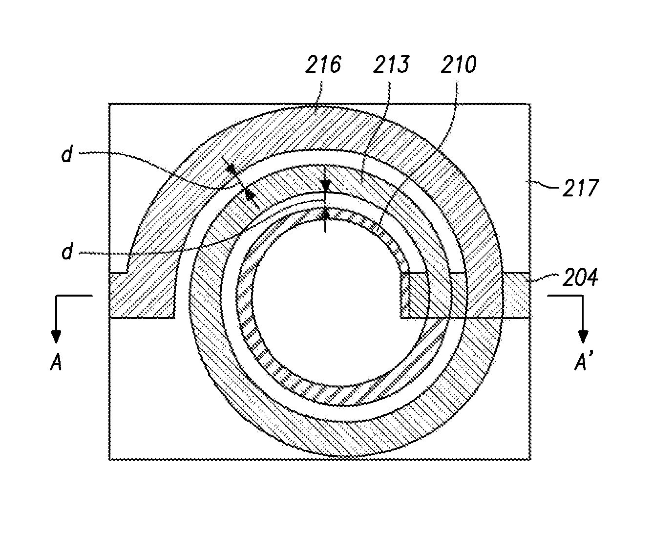
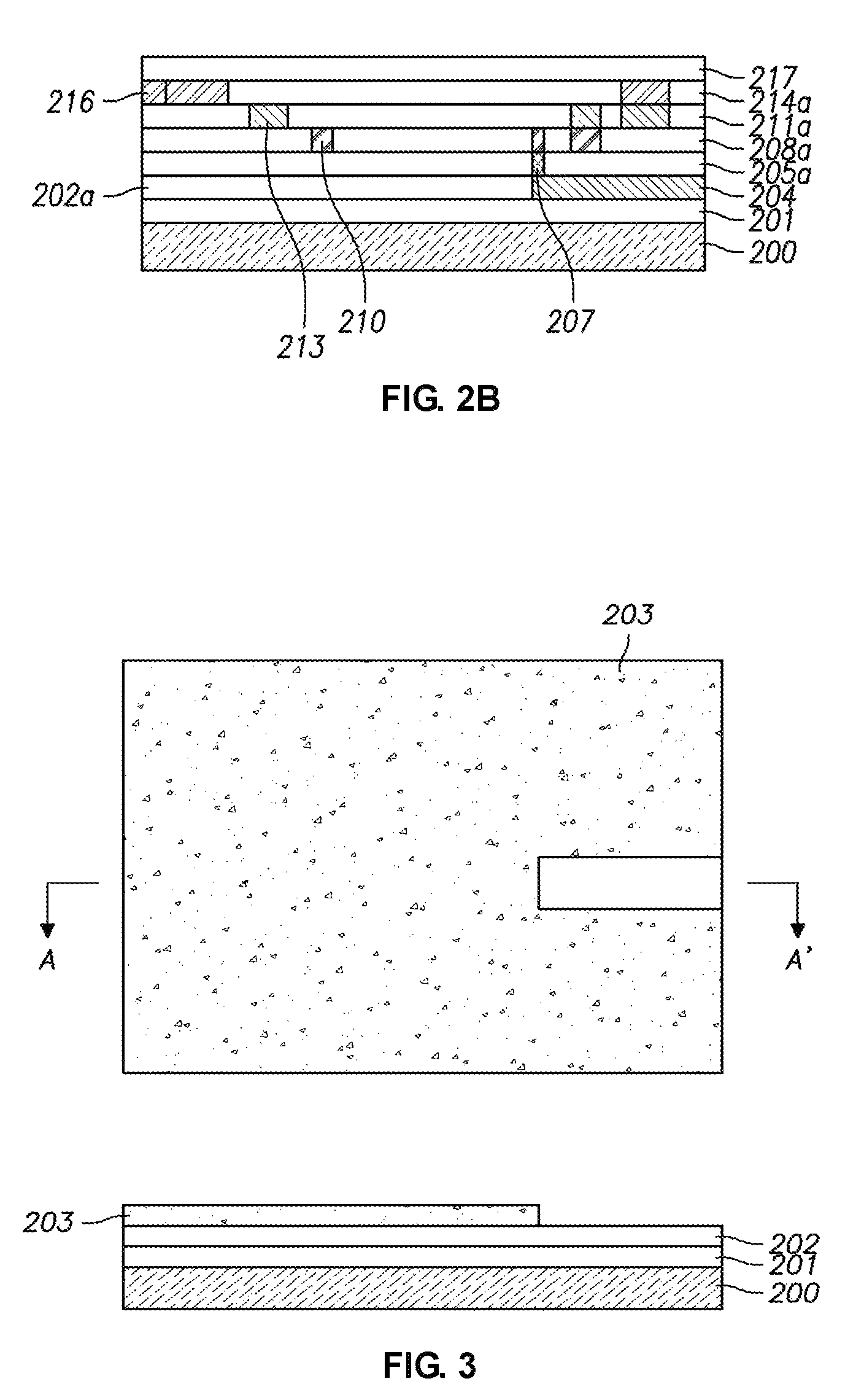
[0019]FIGS. 2A and 2B illustrate a first embodiment of the spiral inductor according of the present invention, wherein FIG. 2A is a projection view showing the spiral inductor structure formed on a semiconductor substrate, and FIG. 2B is a cross-sectional taken the line A-A′ of FIG. 2A.

[0020]In FIGS. 2A and 2B, the spiral inductor comprises a dielectric layer comprising a plurality of layers stacked on a semiconductor substrate 100 and a plurality of curved metal lines 204, 210, 213, and 216, which are formed and disposed between the dielectric layers 201, 202a, 205a, 208a, 211a, 214a, and 217 of the dielectric layer. The curved metal lines 204, 210, 213, and 216 are then and serially connected in order to form a circular spiral shape.

[0021]The metal lines 204, 210, 213, and 216 are serially connected, such that the metal lines 210, 213, and 216 form a circular spiral shape with a line width that gradually becomes increasingly narrow from an outer portion of the circular spiral to a...

embodiment 2

[0052]Another embodiment of a spiral inductor according to the present invention is shown in FIG. 12, wherein the circular spiral is formed with a structure that is the inverse of the structure shown in FIG. 2.

[0053]That is, the first metal line 210 of the center portion of the circular spiral is disposed in the top layer, and the third metal line 216 is disposed in the bottom layer. Thus, the circular spiral is formed with a cone shape.

[0054]Accordingly, a circular spiral structure wherein the width of the spiral gradually decreases from a first width in the third metal line 216 disposed at the bottom layer to a second width in the first metal line 210 disposed in the top layer.

[0055]The method for forming the spiral inductor shown in the FIG. 12 is similar to the first embodiment, and differs only in the order that the photo masks for forming the spiral photo resist pattern are used.

[0056]Similarly to the first embodiment described above, in the second embodiment an extra dielectr...

embodiment 3

[0057]FIGS. 13 to 22 are plan views and cross-sectional views illustrating a spiral inductor and method for forming the same according to a third embodiment of the present invention. The spiral inductor according to the third embodiment shown in FIG. 22 is constituted of a circular spiral in an inverse cone shape, similar to the spiral inductor shown in FIG. 2.

[0058]The spiral inductor according to the third embodiment differs in that it has a shape wherein the width of the metal line is increased in a series of steps proceeding from the outer portion of the circular spiral to the center portion of the circular spiral. Hereinafter, the method for forming the spiral inductor according to the third embodiment will be described in detail.

[0059]First, as shown in FIG. 13, a first dielectric layer 401 and a second dielectric layer 402 are sequentially formed on a semiconductor substrate 400, with a first photo resist pattern 403 being formed on the second dielectric layer 402. Subsequent...


PUM

PropertyMeasurementUnit
thicknessaaaaaaaaaa
thicknessaaaaaaaaaa
thicknessaaaaaaaaaa

Abstract

The present invention relates to a spiral inductor for use in a semiconductor device. The spiral inductor comprises a dielectric layer formed of a plurality of layers stacked on a semiconductor substrate, and a plurality of curved metal lines formed in the dielectric layers which are serially connected in order to form a circular spiral shape.

Description

CROSS-REFERENCES AND RELATED APPLICATIONS[0001]This application claims the benefit of Korean Patent Application No. 10-2006-0137301, filed on Dec. 29, 2006, which is hereby incorporated by reference in its entirety.BACKGROUND OF THE INVENTION[0002]1. Field of the Invention[0003]The present invention relates to a semiconductor device. More specifically, the present invention relates to a spiral inductor for a semiconductor device.[0004]2. Discussion of the Related Art[0005]In order to generate inductance in the substrate of a semiconductor, semiconductor devices include inductors, which are generally formed from forming a metal wire into a spiral form. For example, in the configuration shown in FIG. 1, a metal wire 102 is formed into an inductor in a semiconductor substrate 100 by forming a spiral structure from a series of straight lines.[0006]One difficulty in forming the spiral structure using a series of straight lines, however, is that polarization occurs at the edges of the met...

Claims


Application Information

Patent Timeline
Patent Type & Authority Patents(United States)
IPC IPC(8): H01F5/00
CPCH01F17/0013H01F2017/0053H01F2017/0086H01L27/04
Inventor KIM, SUNG SU
Owner DSS TECH MANAGEMENT
Why Eureka
Try Eureka