Method for forming a spiral inductor

a spiral inductors and transformer technology, applied in the direction of transformers/reacts, instruments, magnetic bodies, etc., can solve the problems of not being easily compatible with silicon vlsi processing, the most common structure and method used for fabricating high q value inductors and transformers in hybrid circuits, monolithic microwave integrated circuits, or discreet applications,

Inactive Publication Date: 2005-07-26
BEIJING XIAOMI MOBILE SOFTWARE CO LTD
View PDF8 Cites 32 Cited by
  • Summary
  • Abstract
  • Description
  • Claims
  • Application Information

AI Technical Summary

Benefits of technology

[0009]Accordingly, in a first aspect of the invention, a method is provided for forming a spiral inductor on a substrate, the method including a step of providing the substrate, the method characterized by: a step of providing the spiral inductor on the substrate so as to have at least one turn made up of at least two interwoven or crisscrossed smaller-width turns.

Problems solved by technology

Implementing high quality factor (called high Q value) inductors that operate at high radio frequencies remains problematic in silicon-based very large scale integration (VLSI) integrated circuit semi-conductor chips.
Most structures and methods used for fabricating high Q value inductors and transformers in hybrid circuits, monolithic microwave integrated circuits, or discreet applications (for example at larger dimensions, with better metals, on lossless substrates, etc.) are not readily compatible with silicon VLSI processing.
Conventional inductors and transformers on silicon, which have strictly planer structures and are fabricated with conventional silicon fabrication processes and material, suffer from several limitations.
First, conventional aluminum interconnect technology has a relatively high metal resistivity and limited metal thickness, both of which lead to a relatively high resistance of the spiral coil.
The high resistivity lowers the quality factor Q, as seen from equation (1), because it contributes to the energy loss per cycle.
Second, magnetic fields are strongly coupled to the silicon substrate, which is a lossy conductor with large skin depth even at radio frequencies.
However, conventional integrated toroidal inductors have comparably small inductance and Q values for a given silicon area relative to the planar spiral inductor configuration, because the area enclosed by wire windings of conventional toroidal inductors is small due to the limit in vertical dimensions of the thin films used in conventional VLSI processing.

Method used


Image

  • Method for forming a spiral inductor
  • Method for forming a spiral inductor
  • Method for forming a spiral inductor

Examples


Embodiment Construction

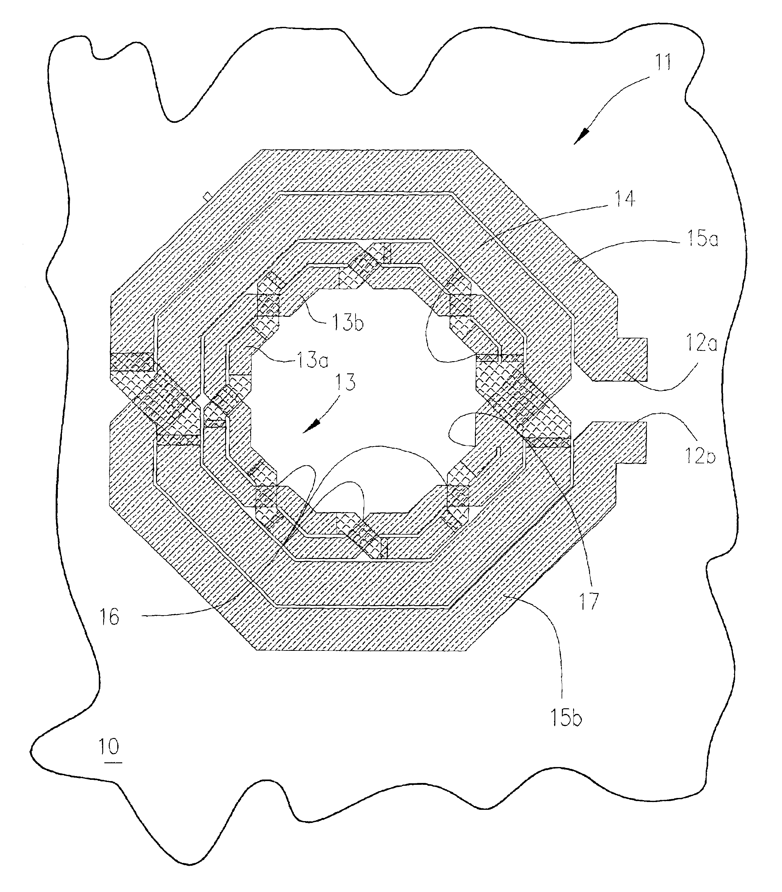
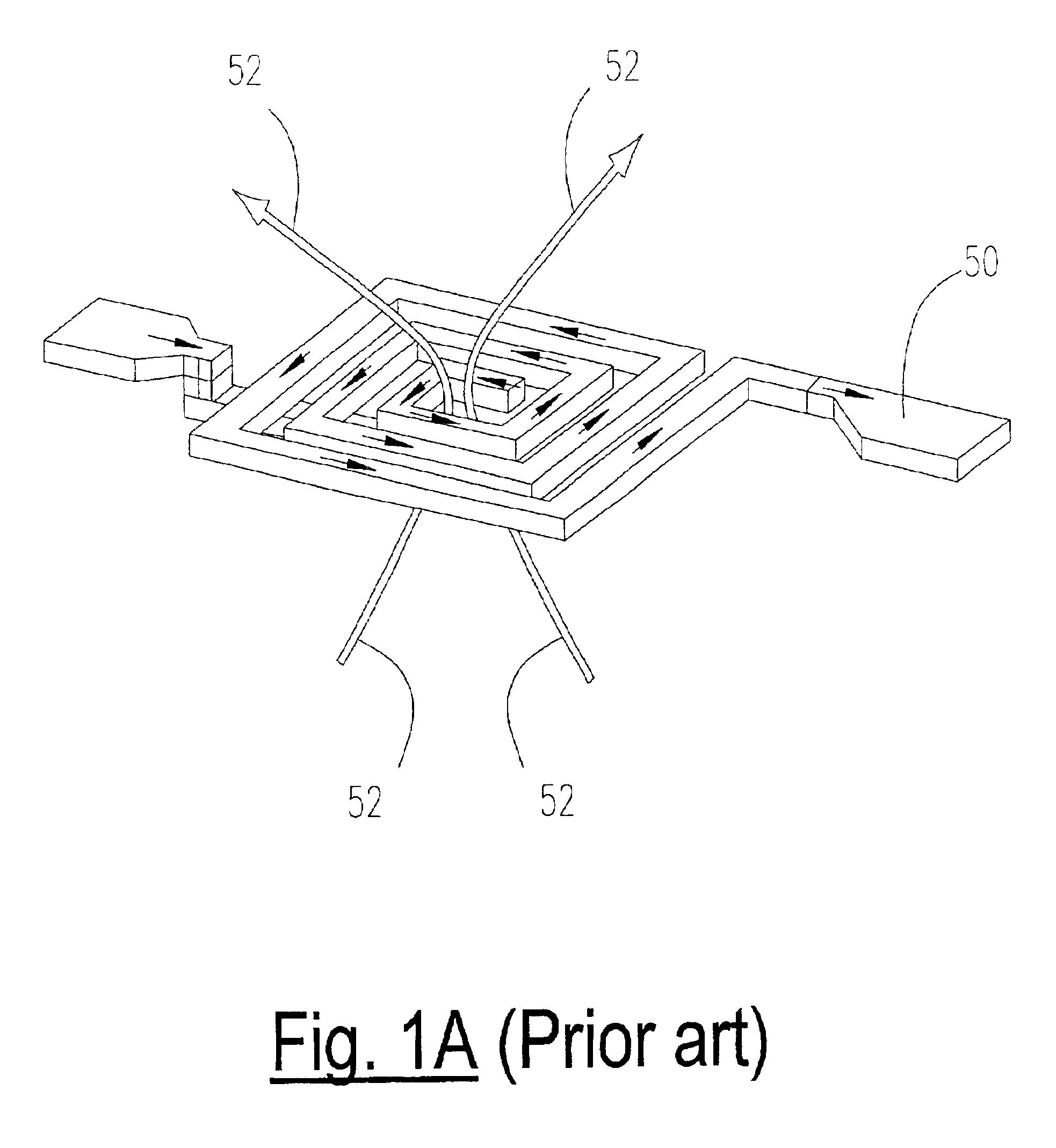
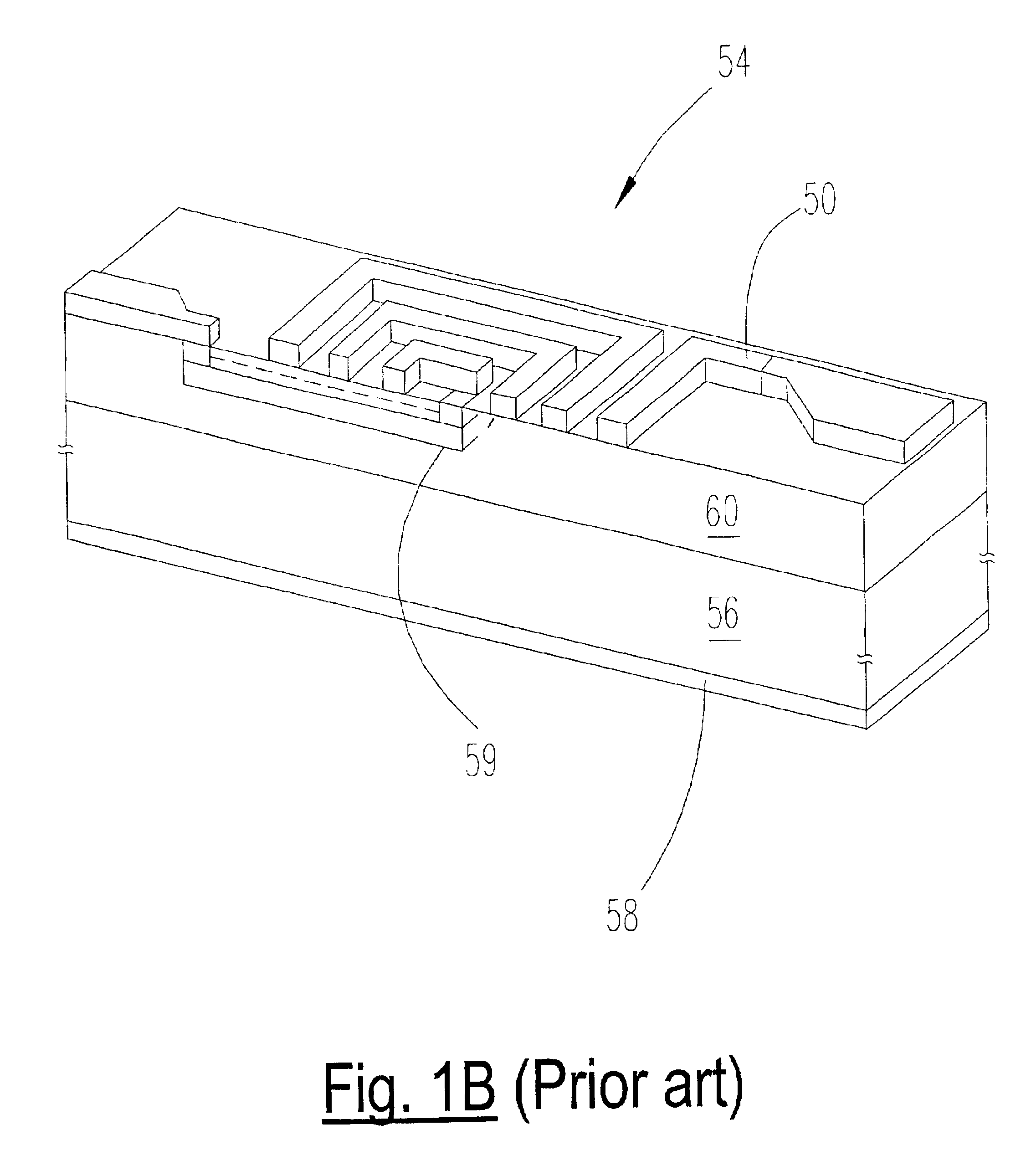
[0027]Referring now to FIG. 2, a spiral inductor 11 according to the invention is shown mounted on a silicon oxide layer 10 (like the silicon oxide layer 60 of FIG. 1B). The spiral inductor11 is itself one or another type of good conductor (typically copper). The spiral inductor does not lie all in one plane (i.e. it is not strictly planar, but only substantially so), since some portions of it pass beneath other portions, and so are buried in the substrate, as illustrated for the prior art spiral inductor of FIG. 1B, showing a buried lead 59 making electrical contact with the innermost part of the spiral inductor 50.

[0028]Referring again to FIG. 2, the substrate 10 of a spiral inductor 11 according to the invention rests on top of a substrate (silicon) such as the substrate 56 of FIG. 1B, which in turn often rests on a conductive ground plane, such as the conductive ground plane 58 of FIG. 1B.

[0029]Still referring to FIG. 2, a spiral inductor 11 according to the invention is an out-...


PUM

PropertyMeasurementUnit
widthaaaaaaaaaa
lengthaaaaaaaaaa
currentaaaaaaaaaa

Abstract

A method for forming a spiral inductor (11) or component of a transformer, compatible with very large scale integrated processing, that achieves a higher Q value without occupying more space by splitting at least one turn (13 51) as two or more crisscrossing or interwoven smaller-width turns (13a 13b 52 53 54 55). The at least one turn (51) may, for example, be split into four turns paired up to provide two pairs of two turns, and the turns of each pair may then be interwoven or crisscrossed, and then the two pairs may also be interwoven or crisscrossed. The splitting of a turn into two or more smaller-width turns results in the current being divided among the smaller-width turns.

Description

FIELD OF THE INVENTION[0001]The invention relates to integrated circuit inductors and transformers, and more particularly to spiral inductors and transformers having a high quality factor (called a Q value).BACKGROUND OF THE INVENTION[0002]Many digital and analog components and circuits have been successfully implemented in the silicon based integrated circuits. Such components include passive devices, such as resistors, capacitors, and inductors.[0003]Implementing high quality factor (called high Q value) inductors that operate at high radio frequencies remains problematic in silicon-based very large scale integration (VLSI) integrated circuit semi-conductor chips. For microwave and wireless communications applications, it is desirable to integrate inductors and transformers monolithically on bulk silicon, silicon on insulator, or silicon on sapphire chips, Gallium-Arsenium or Germanium etc. For these applications, considerable innovation is necessary before adequate values of indu...

Claims


Application Information

Patent Timeline
Patent Type & Authority Patents(United States)
IPC IPC(8): H01F17/00H01F41/04H01L21/02H01L27/08H01F5/00
CPCH01F17/0006H01F41/041H01L27/08H01L28/10H01F5/003Y10T29/49073Y10T29/49069Y10T29/49044Y10T29/49078Y10T29/4902Y10T29/49043Y10T29/49046Y10T29/49048
Inventor VILANDER, ARISVARD, MIKAELHYVONEN, LASSI
Owner BEIJING XIAOMI MOBILE SOFTWARE CO LTD
Why Eureka
Try Eureka