Image sensor with photosensitive thin film transistors

a thin film transistor and image sensor technology, applied in the field of image sensors, can solve the problems of increasing manufacturing costs, difficult assembly of arrays, and not disclosed use of tfts exclusively for image sensors, and achieve the effect of increasing photosensitivity

a thin film transistor and image sensor technology, applied in the field of image sensors, can solve the problems of increasing manufacturing costs, difficult assembly of arrays, and not disclosed use of tfts exclusively for image sensors, and achieve the effect of increasing photosensitivity

US7023503B2Inactive Publication Date: 2006-04-04APPLE INC

Image

  • Image sensor with photosensitive thin film transistors
  • Image sensor with photosensitive thin film transistors
  • Image sensor with photosensitive thin film transistors

Examples


Embodiment Construction

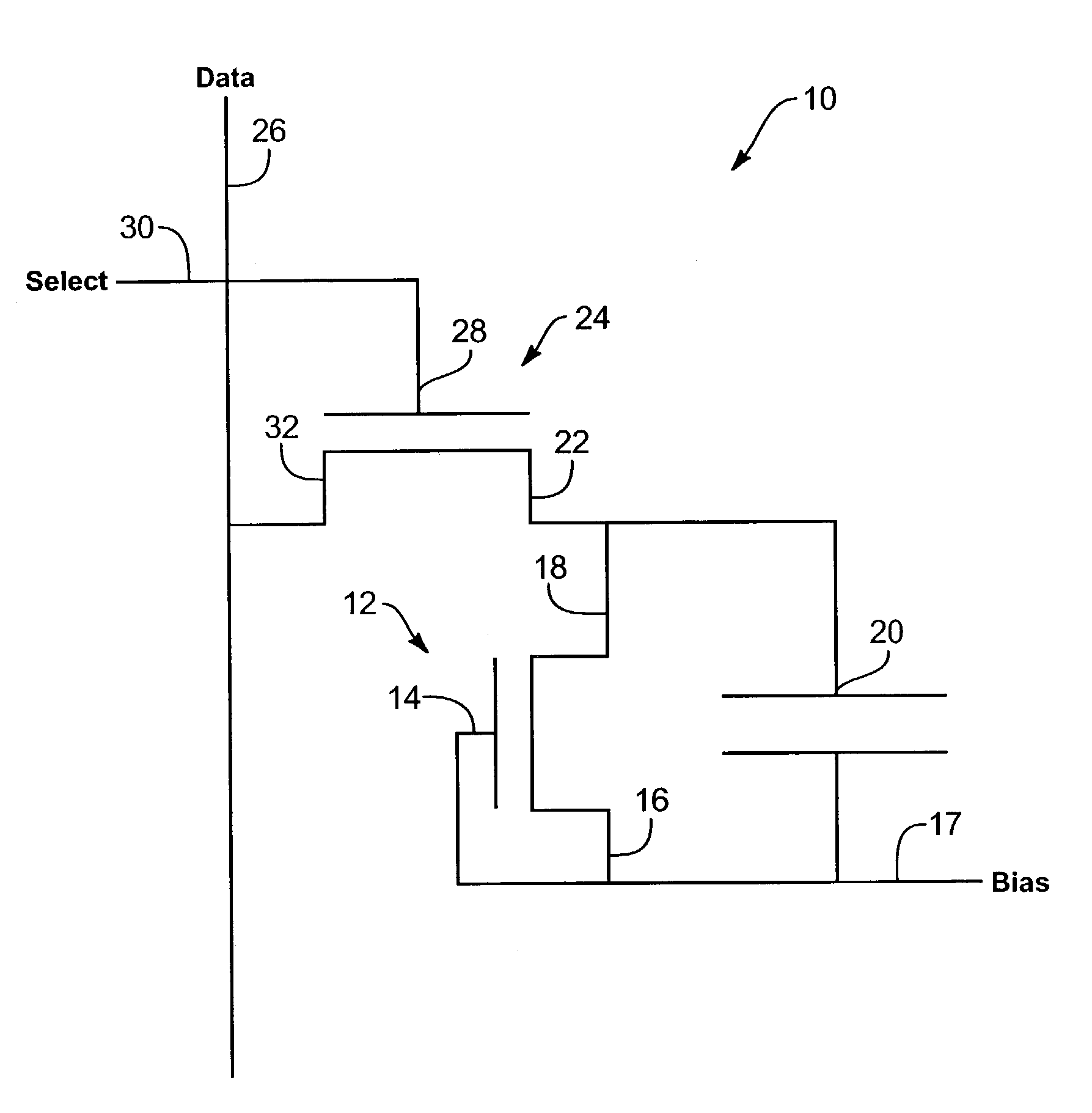
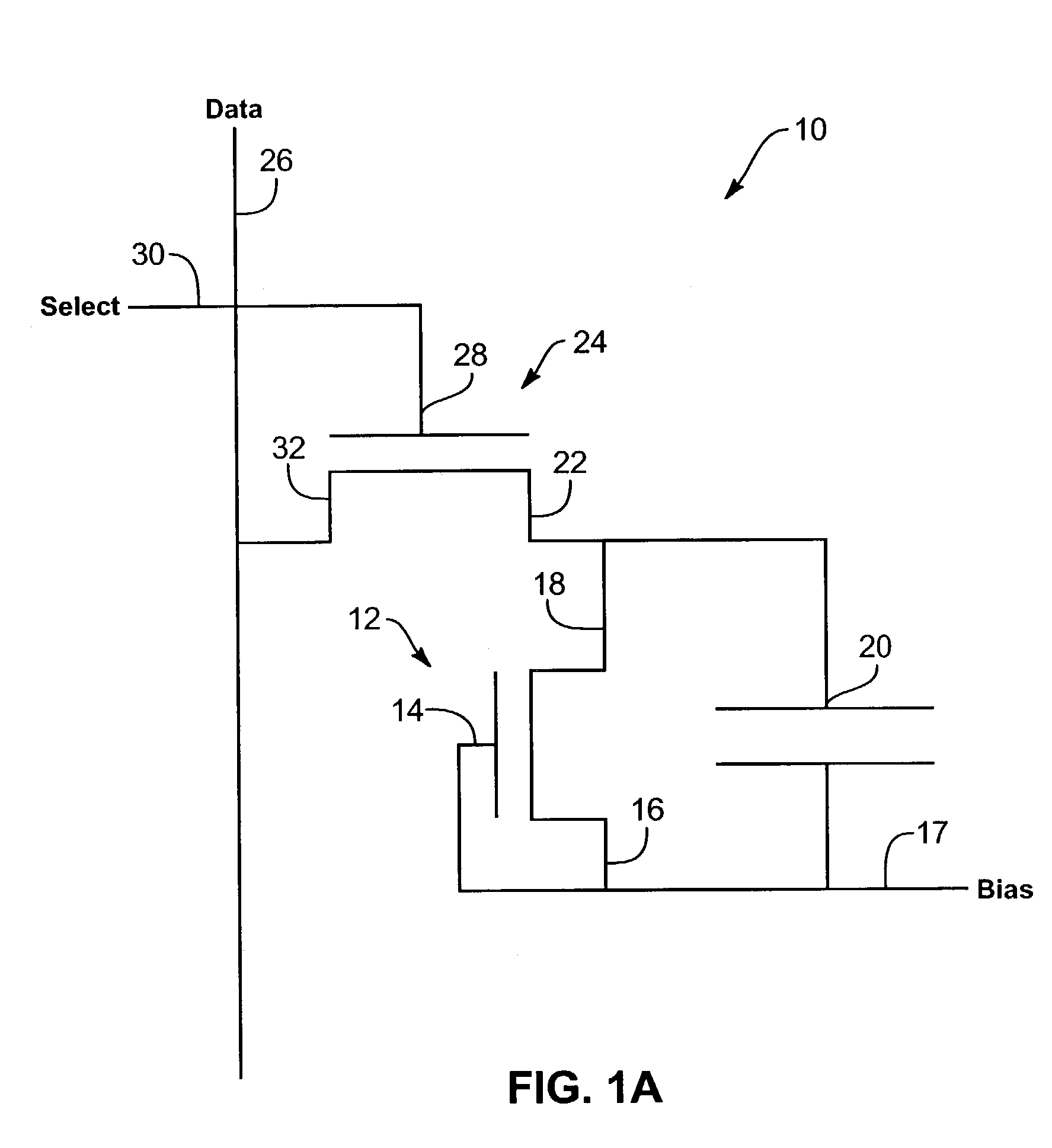
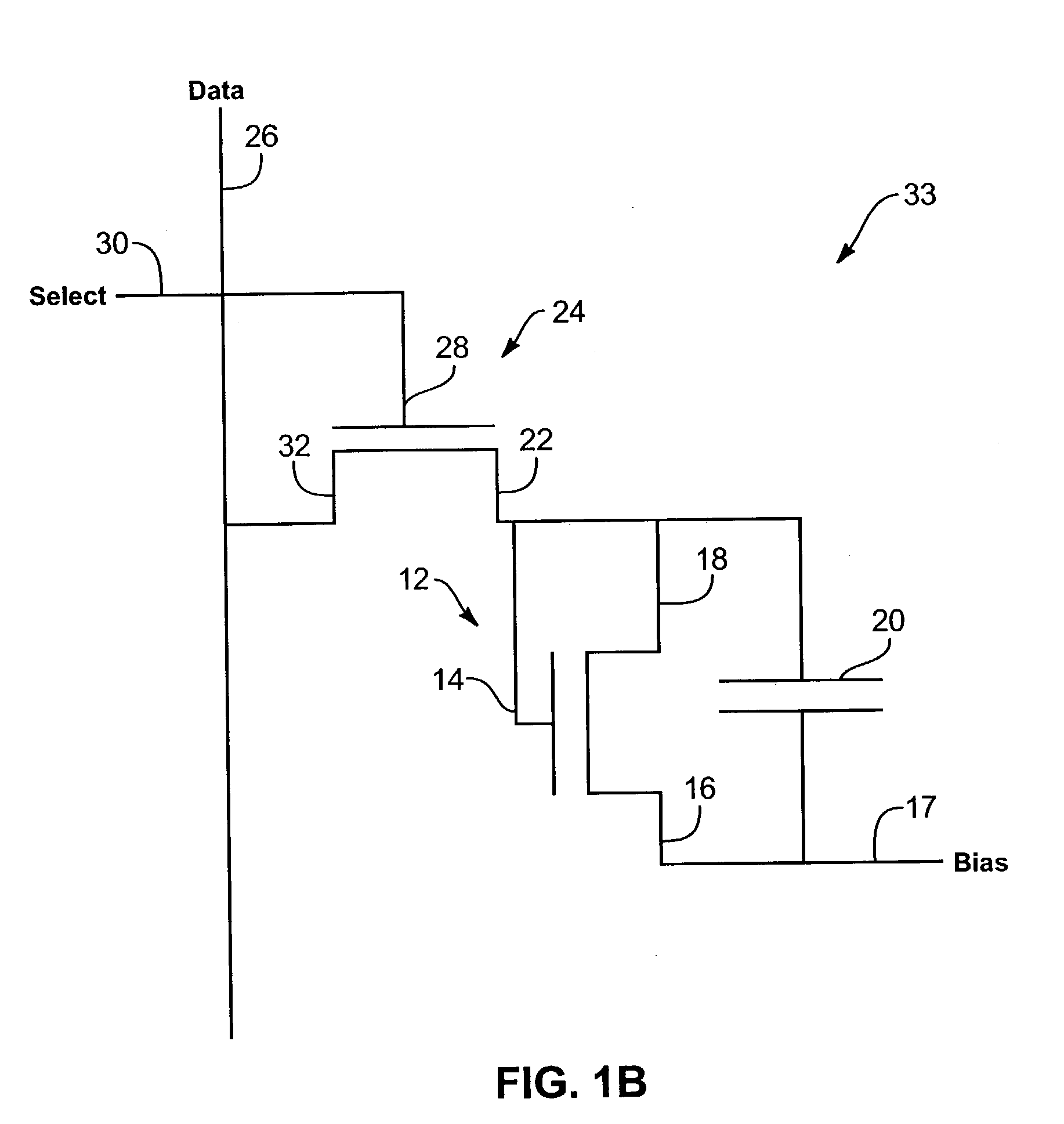
[0022]Reference is now made to the figures in which like reference numerals refer to like elements. For clarity, the first digit or digits of a reference numeral indicates the figure number in which the corresponding element is first used.

[0023]Throughout the specification, reference to ā€œone embodimentā€ or ā€œan embodimentā€ means that a particular described feature, structure, or characteristic is included in at least one embodiment of the present invention. Thus, appearances of the phrases ā€œin one embodimentā€ or ā€œin an embodimentā€ in various places throughout this specification are not necessarily all referring to the same embodiment.

[0024]Furthermore, the described features, structures, or characteristics may be combined in any suitable manner in one or more embodiments. Those skilled in the art will recognize that the invention can be practiced without one or more of the specific details, or with other methods, components, materials, etc. In other instances, well-known structures, ...


PUM

PropertyMeasurementUnit
temperaturesaaaaaaaaaa
wavelengthaaaaaaaaaa
photocurrentaaaaaaaaaa

Abstract

An image sensor array includes image sensors having photo TFTs to generate photocurrent in response to received images. The photo TFTs each have their respective gate electrodes shorted to source electrodes to increase generated photocurrent. Storage capacitors are coupled to each photo TFT and discharged upon generation of a photocurrent. Each storage capacitor is coupled to a readout TFT that passes a current from the storage capacitor to a data line. Data lines indicate location of the received image on the image sensor array.

Description

RELATED APPLICATIONS[0001]This application is a continuation-in-part and claims the benefit under 35 U.S.C. § 120 of U.S. patent application Ser. No. 10 / 217,798, filed Aug. 12, 2002, and U.S. patent application Ser. No. 10 / 307,106, filed Nov. 27, 2002. In addition, this application claims the benefit under 35 U.S.C. § 19(e) of U.S. Provisional Patent Application No. 60 / 359,263, filed Feb. 20, 2002.TECHNICAL FIELD[0002]The present invention relates to image sensors and, more specifically, to flat panel image sensors employing photosensitive thin film transistors.BACKGROUND OF THE INVENTION[0003]Flat panel image sensors are commercially successful products that are able to effectively detect electromagnetic radiation in and near the visible light spectrum. Flat panel image sensors are fabricated by depositing and patterning various metals, insulators, and semiconductors on glass substrates as is done in flat panel displays. Such sensors commonly employ photosensitive elements, such as...

Claims


Application Information

Patent Timeline
04 Apr 2006
Publication
US7023503B2
IPC
G02F1/136; G09G3/20; H01L27/00; H01L29/04; H01L27/14; H01L27/146
CPC
H01L27/14609; H01L27/14643
Inventors
DEN BOER, WILLEM