Method of producing a semiconductor device

a technology of semiconductor devices and semiconductors, applied in the direction of semiconductor devices, basic electric elements, electrical appliances, etc., can solve the problems of reducing achieve the effects of improving the reliability of gate electrodes, reducing the on-resistance of transistors, and reducing the cost of transistors

Inactive Publication Date: 2006-04-11
DENSO CORP
View PDF9 Cites 11 Cited by
  • Summary
  • Abstract
  • Description
  • Claims
  • Application Information

AI Technical Summary

Benefits of technology

[0011]In view of the above-mentioned problems, it is an object of the present invention to provide a superior semiconductor device having an improved reliability with suppression of increase in the ON-resistance from the desired value.
[0012]Another object of the present invention is to provide a superior method of producing a semiconductor device.
[0015]In the above device, concentration of electric field applied to the oxide film on the sidewalls at the gate lead wiring region is comparatively suppressed, i.e., the electric field intensity around a corner is suppressed to increase. Therefore, the reliability of the gate electrode is improved.
[0017]Thus, the reliability of the gate electrode is improved with suppression of increase in ON-resistance of the transistor from the desired value.
[0027]In the above device, concentration of electric field applied to the oxide film on the sidewalls at the gate lead wiring region is comparatively suppressed, so that the reliability of the gate electrode is improved. Moreover, since the oxide film on the sidewalls at the cell region is comparatively thin, mutual conductance remains comparatively high. Accordingly, ON-resistance of a transistor is limited to increase. Thus, the reliability of the gate electrode is improved with suppression of increase in ON-resistance of the transistor from the desired value.

Problems solved by technology

Therefore, this electric field concentration reduces the reliability of the gate electrode.

Method used


Image

  • Method of producing a semiconductor device
  • Method of producing a semiconductor device
  • Method of producing a semiconductor device

Examples


first embodiment

[0055](First Embodiment)

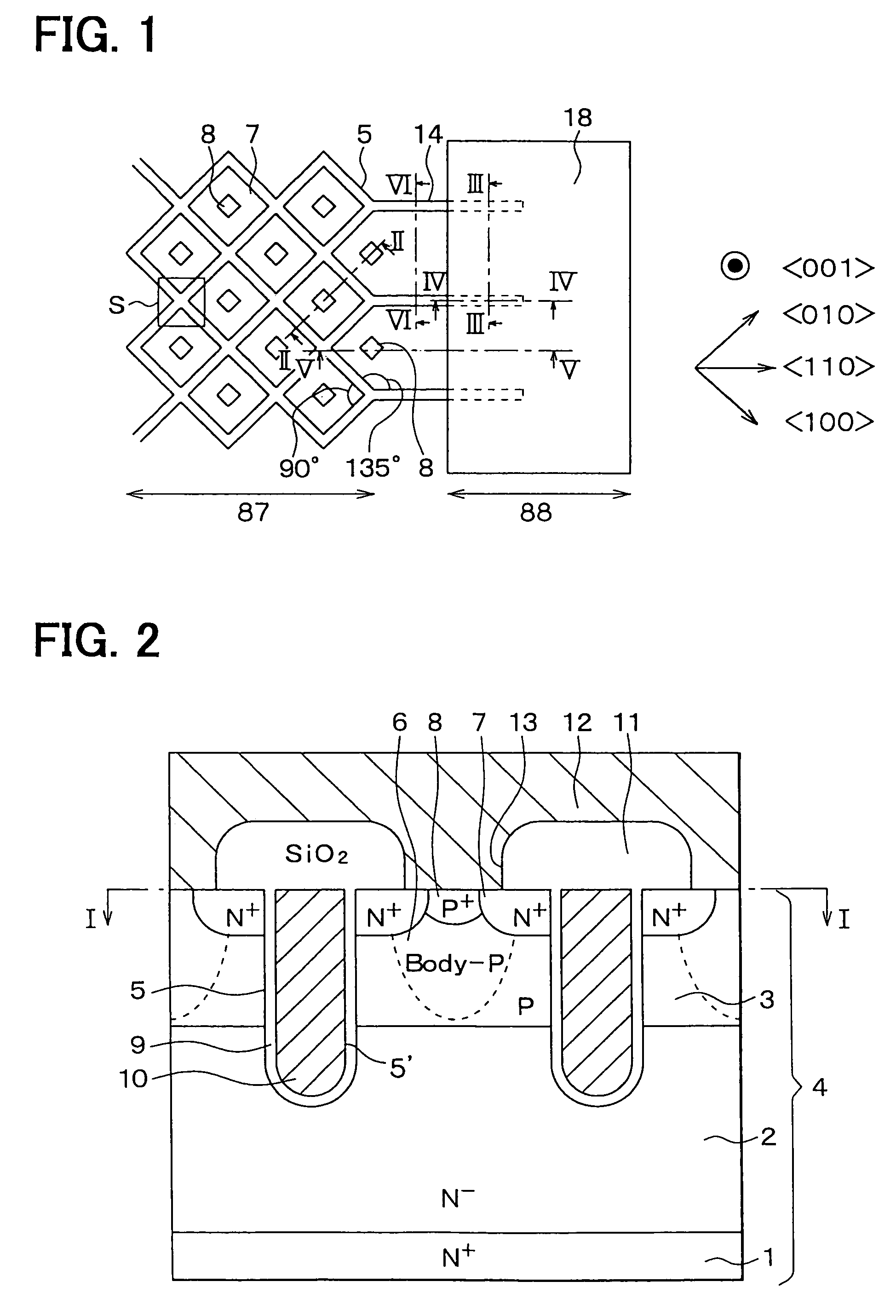
[0056]As shown in FIGS. 1 and 2, a semiconductor device according to the first embodiment of the present invention includes a diffused metal-oxide semiconductor i.e., DMOS. Here, FIG. 1 shows a top view of a substrate 4 on arrow I—I in FIG. 2 for clarity, i.e., FIG. 1 shows the top view of the substrate 4 with removing a layer-to-layer insulation film 11 and a metal electrode 12 from the device. Following plan view in each drawing also shows a top view of a substrate, similar to FIG. 1. This semiconductor device includes a semiconductor substrate 4 having an N+ type substrate 1, an N− type drift layer 2 on the N+ type substrate 1, P type base region 3 on the N− type drift layer 2. The substrate 4 is made of silicon. An impurity diffusion concentration of the N+ type substrate 1 is, for example, 1×1019 cm−3, that of the N− type drift layer 2 is, for example, 1×1016 cm−3, and that of the P type base region 3 is, for example, 1×1018 cm−3.

[0057]The semiconductor ...

second embodiment

[0101](Second Embodiment)

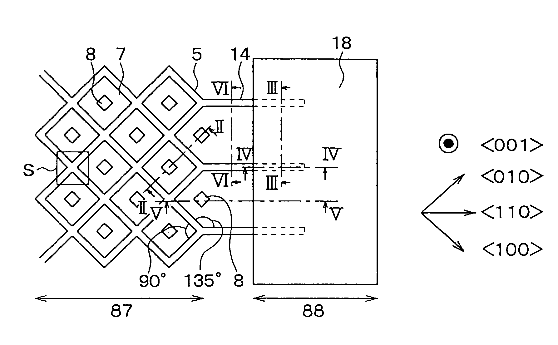
[0102]A semiconductor device according to the second embodiment has the cell region 87 and the gate lead wiring region 88, as shown in FIG. 7. The trench 14 extends from the cell region 87 to the gate lead wiring region 88. Each mesh has a parallelogram having trench sides 5a extending parallel to the axis and trench sides 5b extending perpendicularly to the axis, i.e., extending parallel to the axis. Here, the trench sides 5a, 5b show a top view of the sidewalls of the trench 5.

[0103]At the cell region 87, a pair of sidewalls of the trench 5 are composed of the (010) and (0{overscore (1)}0) planes, the sidewalls including the trench sides 5a (i.e., the sidewalls of the trench sides 5a have the (010)-oriented planes). Another pair of sidewalls of the trench 5 are composed of the (110) and ({overscore (1)}{overscore (1)}0) planes, the sidewalls including the trench sides 5b (i.e., the sidewalls of the trench sides 5b have the (110)-oriented planes). At the...

third embodiment

[0108](Third Embodiment)

[0109]As shown in FIG. 8, a semiconductor device according to the third embodiment has the cell having a hexagon mesh.

[0110]At the cell region 87, each cell has a hexagon mesh including trench sides 31a extending parallel to the axis, trench sides 31b extending parallel to the axis, and trench sides 31c extending parallel to the axis. Therefore, the trench sides 31c are parallel to the trench 14 at the gate lead wiring region 88.

[0111]The trench side 31a intersects with the trench side 31b at an angle of 90°, and the trench side 31c intersects with the trench side 31a, 31b at an angle of 135°. A width 32 of the trench 31 is in a range between 0.5 μm and 1.0 μm. The length of the trench side 31c on the surface of the semiconductor substrate 4 is in a range between 0.5 μm and 1.0 μm, which is substantially the same as the width 32 of the trench 31.

[0112]The trench 14 formed at the gate lead wiring region intersects with the trench side 31a, 31b at the cell r...


PUM


Abstract

A semiconductor device includes a semiconductor substrate, a cell region in a surface portion of the substrate for operating as a transistor, a gate lead wiring region having a gate lead pattern on the substrate, a trench in the surface portion of the substrate extending from the cell region to the gate lead wiring region, an oxide film on an inner surface of the trench, and a gate electrode in the trench insulated with at least the oxide film from the substrate. A speed of formation of a main portion of the sidewalls of the trench at the gate lead wiring region is greater than that of a main portion of the sidewalls of the trench at the cell region, so that a thickness of the oxide film at the gate lead wiring region is greater than that at the cell region.

Description

CROSS REFERENCE TO RELATED APPLICATION[0001]This application is a division of application Ser. No. 10 / 635,490 filed on Aug. 7, 2003, which is based on Japanese Patent Application No. 2002-241859 filed on Aug. 22, 2002, the disclosure of which is incorporated herein by reference.FIELD OF THE INVENTION[0002]The present invention relates to a semiconductor device and a method of producing the same, and particularly to a semiconductor device having a trench gate structure and a method of producing the same.BACKGROUND OF THE INVENTION[0003]According to a related art, some semiconductor devices have a trench gate structure to control a current flowing between a source and a drain thereof. These semiconductor devices as a trench gate type transistor have a structure shown in FIG. 25. Here, FIG. 25 shows a top view of a substrate 4 on arrow XXV—XXV in FIG. 26A for clarity, i.e., FIG. 25 shows the top view of the substrate 4 with removing a layer-to-layer insulation film 11 from the device. ...

Claims


Application Information

Patent Timeline
Patent Type & Authority Patents(United States)
IPC IPC(8): H01L21/336H01L29/78H01L21/28H01L29/06H01L29/12H01L29/51H01L29/739
CPCH01L21/28194H01L29/045H01L29/0696H01L29/7813H01L29/513H01L29/518H01L29/7397H01L29/7811H01L21/28202H01L29/1095H01L29/4238
Inventor AOKI, TAKAAKITSUZUKI, YUKIO
Owner DENSO CORP
Why Eureka
Try Eureka