Electrically tunable quantum dots and methods for making and using same

a quantum dot and electric tunable technology, applied in the field of quantum dots, can solve the problems of physical limitations, inability to achieve wavelength tunability at the “pixel level” by these methods, and difficulty in mass production integration

Inactive Publication Date:
View PDF0 Cites 63 Cited by
  • Summary
  • Abstract
  • Description
  • Claims
  • Application Information

AI Technical Summary

Benefits of technology

[0011]The method may include the steps of forming at least two epitaxial grown structures, wherein the epitaxial grown structures include at least two GaAs layers sandwiching a plurality of AlGaAs / GaAs multi-quantum wells, spin coating a mask onto the epitaxial grown structure, wherein the mask includes one selected from micro or nano spheres, or other shapes, evaporating a gate metal layer onto the mask, wherein the spherical shape of the mask substantially prevents formation of a continuous gate metal layer, lifting off at least a portion of the gate metal by dissolving the spheres, self isolating the gate metal, and evaporating a top contact onto one of the epitaxial grown layers.

Problems solved by technology

However, wavelength tunability at a “pixel level” cannot be achieved by these methods.
Such integration is difficult to develop for mass production, and has several physical limitations.
Such difficulties are due, in part, to the absence of an effective multi-level heterogeneous integration method.
More fundamentally, such difficulties are due, in part, to physical separation of the filter and detector, which makes the broadband detector more vulnerable to interference, such as pixel-to-pixel crosstalk, wavelength suppression, and the like.
This vulnerability becomes more significant as electrical interconnections and / or electronic components are placed between the elements of the filter and the elements of the detector.
Additionally, thermal, mechanical, and electrical incompatibilities between the material of the filter and the material of the detector may limit the operation of the device to undesirably narrow temperature, acceleration, and voltage ranges.
Unfortunately, this bandwidth is not narrow enough for many applications, and it cannot be easily tuned.

Method used


Image

  • Electrically tunable quantum dots and methods for making and using same
  • Electrically tunable quantum dots and methods for making and using same
  • Electrically tunable quantum dots and methods for making and using same

Examples


Embodiment Construction

[0026]It is to be understood that the figures and descriptions of the present invention have been simplified to illustrate elements that are relevant for a clear understanding of the present invention, while eliminating, for purposes of clarity, many other elements found in a tunable detector apparatus, system, and method. Those of ordinary skill in the art will recognize that other elements are desirable and / or required in order to implement the present invention. However, because such elements are well known in the art, and because they do not facilitate a better understanding of the present invention, a discussion of such elements is not provided herein.

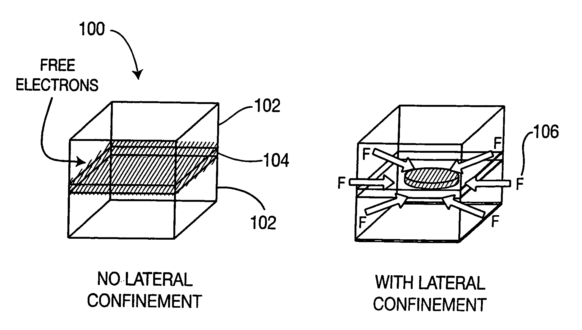
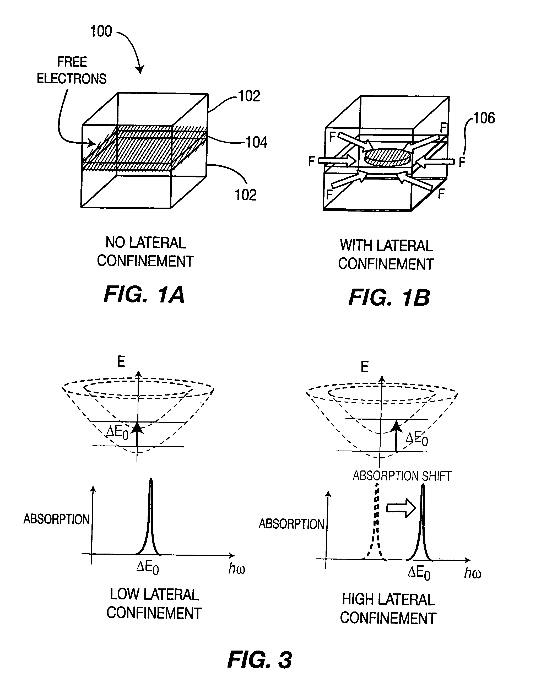
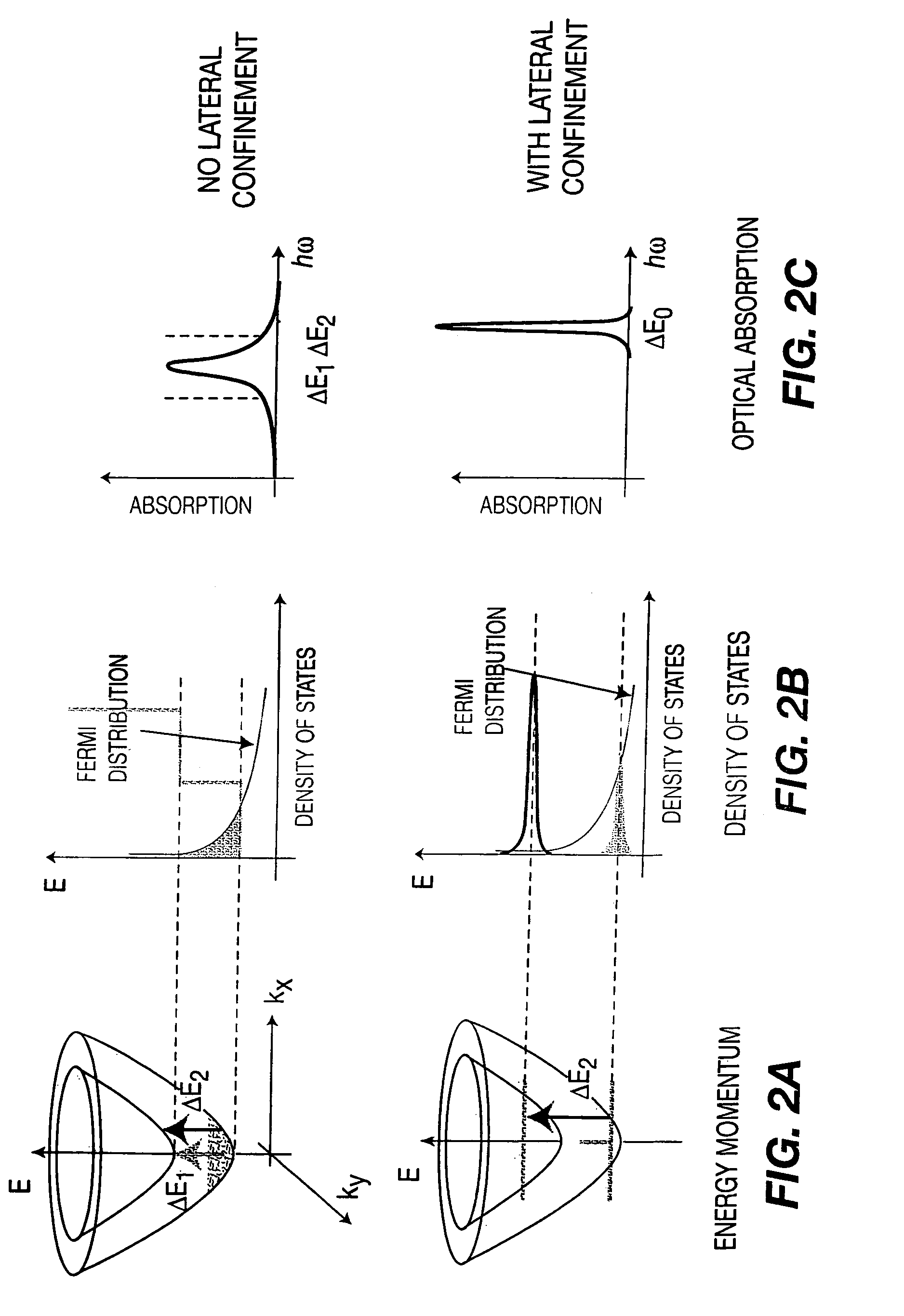
[0027]According to an aspect of the present invention a method and apparatus to induce a lateral electric field on a conventional quantum well structure, which lateral field results in a lateral energy confinement that breaks the in-plane periodic potential, and thereby collapses the energy “bands” into energy “states” may be prov...


PUM


Abstract

A method of fabricating a tunable quantum dot apparatus, comprising: forming multi-quantum wells sandwiched substantially between at least two barrier layers; spin coating a non-continuous mask onto at least one of said barrier layers; forming a gate material onto the mask, wherein the non-continuity of the mask substantially prevents formation of a continuous gate material layer; lifting off at least a portion of the gate material; self isolating the gate material; and, forming a top contact onto at least a portion of said barrier layers

Description

CROSS REFERENCE TO RELATED APPLICATIONS[0001]This Application claims the benefit of priority to now abandoned U.S. Provisional Patent Application Ser. No. 60 / 403,927, entitled “Fabrication of Electrically Tunable Quantum Dots”, filed Aug. 15, 2002, the entire disclosure of which is hereby incorporated by reference as if being set forth herein in its entirety.FIELD OF THE INVENTION[0002]The present invention is directed generally to a method and apparatus relating to quantum dots, and, more particularly, to a method and apparatus for a self-aligned, self-isolating realization of quantum dots by which three-dimensional quantum confinement can be electrically tuned.DESCRIPTION OF THE BACKGROUND OF THE INVENTION[0003]A system, such as an infrared system, may realize wavelength selectivity by, for example, filtering selected photons, or, for example, by selective detection of photons having a particular wavelength. Further, a system, such as an infrared system, may realize wavelength tun...

Claims


Application Information

Patent Timeline
Patent Type & Authority Patents(United States)
IPC IPC(8): H01L29/06H01L21/335H01L29/12H01L29/775
CPCB82Y10/00H01L29/127H01L29/775H01L29/66469Y10S977/774
Inventor MOHSENI, HOOMANCHAN, WINSTON KONG
Why Eureka
Try Eureka