

Probe mark reading device and probe mark reading method
- Summary
- Abstract
- Description
- Claims
- Application Information
AI Technical Summary
Benefits of technology
Problems solved by technology
Method used
Image

Examples
Embodiment Construction
[0087]The following is a detailed description, with reference to the appended drawings, of a preferred embodiment of the present invention.
[0088]1. Overall Configuration
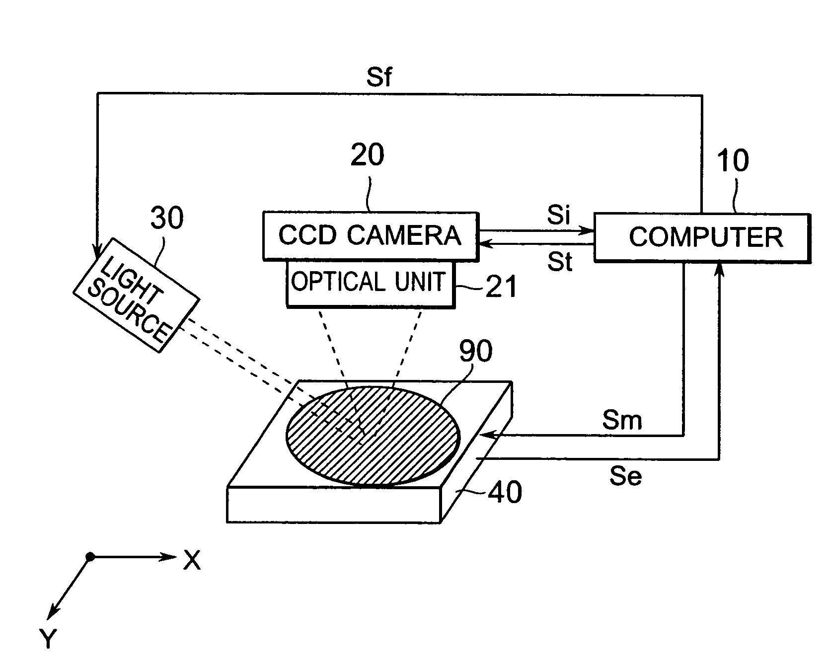
[0089]FIG. 1 is a block view showing a configuration for a probe mark reading device of an embodiment of the present invention. The probe mark reading device for reading probe marks formed on electrode pads of semiconductor chips contained on a semiconductor wafer 90 comprises a CCD camera 20 for taking images of the semiconductor wafer 90, an optical unit 21 for optically enlarging an image of a location to be photographed by the CCD camera 20, a light source 30 for illuminating the location to be photographed by the CCD camera 20, an X-Y stage 40 including a mounting table mounted with the semiconductor wafer 90 and being capable of changing a position to be photographed by the CCD camera 20 by moving the mounting table in an X-direction and a Y-direction, and a computer 10 for controlling the above. It is taken th...
PUM
 Abstract
Description
Claims
Application Information