Method for producing a polycrystalline silicon, polycrystalline silicon and solar cell

a technology of polycrystalline silicon and solar cells, applied in the direction of final product manufacture, crystal growth process, climate sustainability, etc., can solve the problems of deterioration of various performances and deterioration of carrier lifetime, and achieve the effect of not almost deteriorating conversion efficiency and optical and electrical properties such as minority carrier lifetimes

Inactive Publication Date: 2006-04-18
KYOCERA CORP
View PDF14 Cites 3 Cited by
  • Summary
  • Abstract
  • Description
  • Claims
  • Application Information

AI Technical Summary

Benefits of technology

[0007]It is an object of the present invention to provide a new polycrystalline silicon wherein the optical and electrical properties such as minority-carrier lifetimes are not almost deteriorated and thus, the various device performances such as conversion efficiency are not almost deteriorated.
[0013]In this point of view, the inventors had much studied to find out the fact that the minority-carrier lifetime in the polycrystalline silicon can be developed by adding Ga dopant therein, instead of conventional B dopant. Therefore, if Ga dopant is incorporated in the polycrystalline silicon by a given amount to be employed as a substrate of a solar cell, the optical and electrical properties are not almost deteriorated due to the dopant, and thus, the various performances such as conversion efficiency of the solar cell can be developed.
[0015]In another embodiment of the present invention, in the addition of the Ga dopant into the silicon raw material, oxygen-including compound is also added into the silicon raw material. In this case, the oxygen content of the intended polycrystalline silicon can be increased to some level, and thus, the crystal strength of the polycrystalline silicon can be developed. As a result, even though a thinner substrate is made from the polycrystalline silicon, the mechanical strength of the substrate can be much developed.

Problems solved by technology

In this case, however, the carrier lifetime may be deteriorated and various performances may be deteriorated under sunlight.

Method used


Image

  • Method for producing a polycrystalline silicon, polycrystalline silicon and solar cell

Examples


example 1

[0027]4.5 kg of silicon raw material and 0.25 g (2×10⁻³ atomic %) of gallium metal were charged into a quartz crucible of which inner surface is coated with a mold lubricant. The mixture was heated to 1550° C. under an Ar gas atmosphere to melt the silicon raw material. After the melting, the crucible was cooled down at a rate of 1° C. / min to crystallize the melted silicon raw material. The resultant crystalline silicon ingot was cut off, and then, the cross section of the silicon ingot was observed. As a result, it was confirmed that in the silicon ingot, polycrystalline boundaries were created vertically, and thus, silicon crystals were created in columnar.

[0028]Then, the polycrystalline silicon ingot was cut off with a wire saw to make a substrate with a thickness of 300 μm. In this case, the resistivity of the polycrystalline silicon ingot was within a range of about 1-2 Ωcm, and decreased in the upper portion thereof.

[0029]In order to remove the slice damaged layer formed at th...

example 2

[0034]A Ga-doped polycrystalline silicon ingot was made in the same manner as in Example 1, and then, cut off with a wire saw to make three substrates with a thickness of 300 μm. The resistivities of the substrates were 2 Ωcm, 1.84 Ωcm and 1.84 Ωcm, respectively.

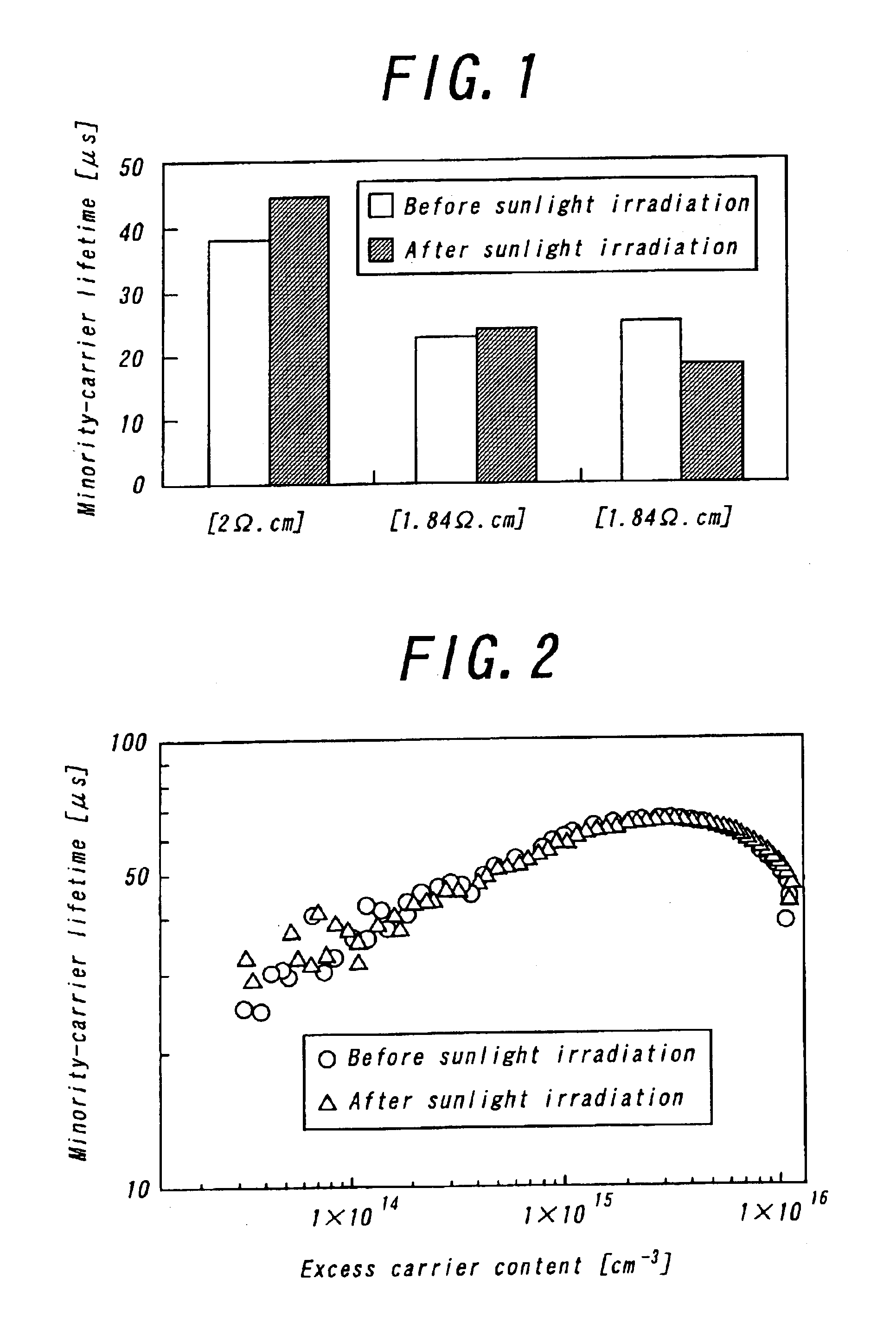
[0035]Then, the substrates were annealed at a temperature of 200° C. for 10 minutes under an inert gas atmosphere. Thereafter, a simulated-sunlight (spectrum: AM1.5, intensity: 100 m W / cm2) was irradiated onto the substrates for 12 hours by means of the optical conductivity attenuating method to measure the minority-carrier lifetime of the substrates, respectively. The measurement result was drawn in FIG. 1. As is apparent from FIG. 1, the minority-carrier lifetime of the annealed substrates are not almost changed after the long irradiation of 12 hours.

[0036]Then, the relation between the minority-carrier lifetime and the excess carrier contents of the substrates made of the polycrystalline silicon was investigated by means ...

example 3

[0037]4 kg of silicon raw material, 0.25 g (2×10⁻³ atomic %) of gallium metal and a predetermined amount of silicon oxide were charged into the quartz crucible. The mixture was heated and melted and then, a crystalline silicon ingot was made in the same manner as in Example 1. The crystalline silicon ingot was cut off to make a substrate with a thickness of 300 μm. The oxygen content of the substrate was 1018 / cm3, and the yield stress of the substrate at a temperature of 800° C. was 40 MPa. In contrast, the oxygen content of the substrate made in Example 1 was 1016 / cm3, and the yield stress of the substrate was 15 MPa.

[0038]In this way, if the oxygen content of the polycrystalline silicon increases, the crystal strength of the polycrystalline silicon can increase. Therefore, if a thinner substrate is made from the oxygen-including poly-crystalline silicon, the mechanical strength can be enhanced sufficiently.


PUM

PropertyMeasurementUnit
temperatureaaaaaaaaaa
thicknessaaaaaaaaaa
thicknessaaaaaaaaaa

Abstract

Silicon raw material and gallium dopant are charged and mixed in a crucible. The silicon raw material is heated to a predetermined temperature, and melted under an inactive gas atmosphere. The melted silicon raw material is cooled down to be crystallized to make a polycrystalline silicon incorporating the gallium dopant.

Description

BACKGROUND OF THE INVENTION[0001]1. Field of the Invention[0002]This invention relates to polycrystalline silicon which is usable as silicon substrates for solar cells, and a method for producing the polycrystalline silicon.[0003]2. Related Art[0004]From 1995 onward, the global market of solar cells has been largely developed per about 30% every year. In 2001, the worldwide amount of the solar cell production was 390 MWp, which is almost close to 400 MWp. The large development of the global market of solar cells is mainly originated from the development for residential application. As of now, various solar cells are used for various applications, and in 2001, according to Mr. P. Haycock, crystalline silicon solar cells are much used which are made from Cz single crystalline silicon crystal or casted polycrystalline silicon. Therefore, in the global market of solar cells, the ratio of the Cz single crystalline silicon solar cells or the casted polycrystalline silicon solar cells for ...

Claims


Application Information

Patent Timeline
Patent Type & Authority Patents(United States)
IPC IPC(8): C01B33/02C22C29/00C22C35/00C01B15/14C30B11/00C30B29/06H01L21/302H01L21/306H01L21/461H01L31/00H01L31/18
CPCC30B11/00C30B29/06H01L31/182Y02E10/546H01L21/30604Y02P70/50
Inventor SAITO, TADASHI
Owner KYOCERA CORP
Why Eureka
Try Eureka