Semiconductor device and method of manufacturing the same

Inactive Publication Date: 2006-04-18
RENESAS ELECTRONICS CORP
View PDF7 Cites 9 Cited by
  • Summary
  • Abstract
  • Description
  • Claims
  • Application Information

AI Technical Summary

Benefits of technology

[0016]According to the present invention, junction

Problems solved by technology

Nevertheless it is difficult to practically apply the method of manufacturing an N-MOS transistor described in this document as it is to manufacturing of a P-MOS transistor.
This leads to a drawback that a material having a large diffusion coefficient may often be emplo

Method used


Image

  • Semiconductor device and method of manufacturing the same
  • Semiconductor device and method of manufacturing the same
  • Semiconductor device and method of manufacturing the same

Examples


examples

[0067]The present invention will be described in further details here below referring to examples, however it is to be understood that the present invention is not limited thereto.

[0068]An example of the present invention will be described as under referring to FIG. 1A through FIG. 9.

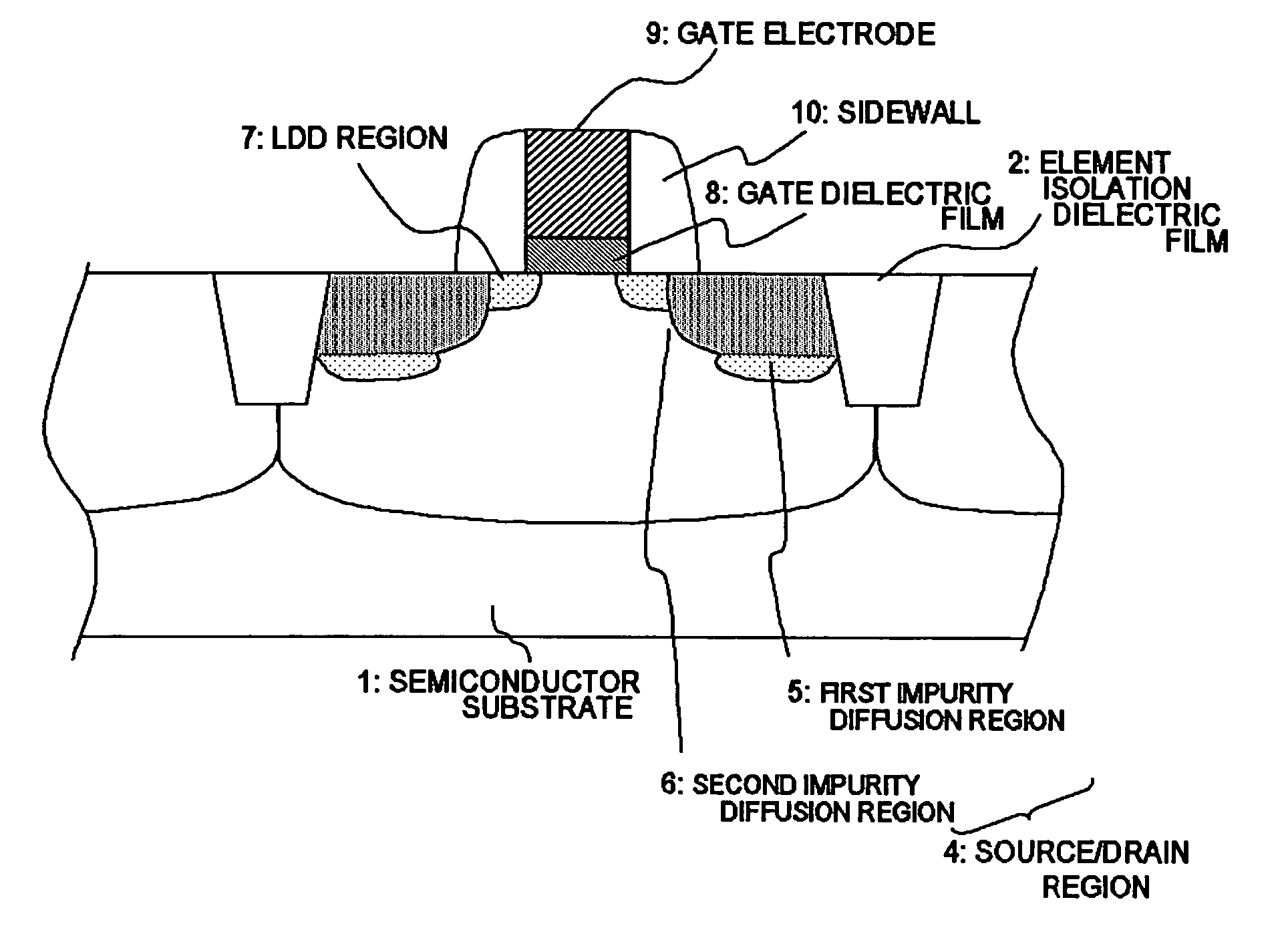
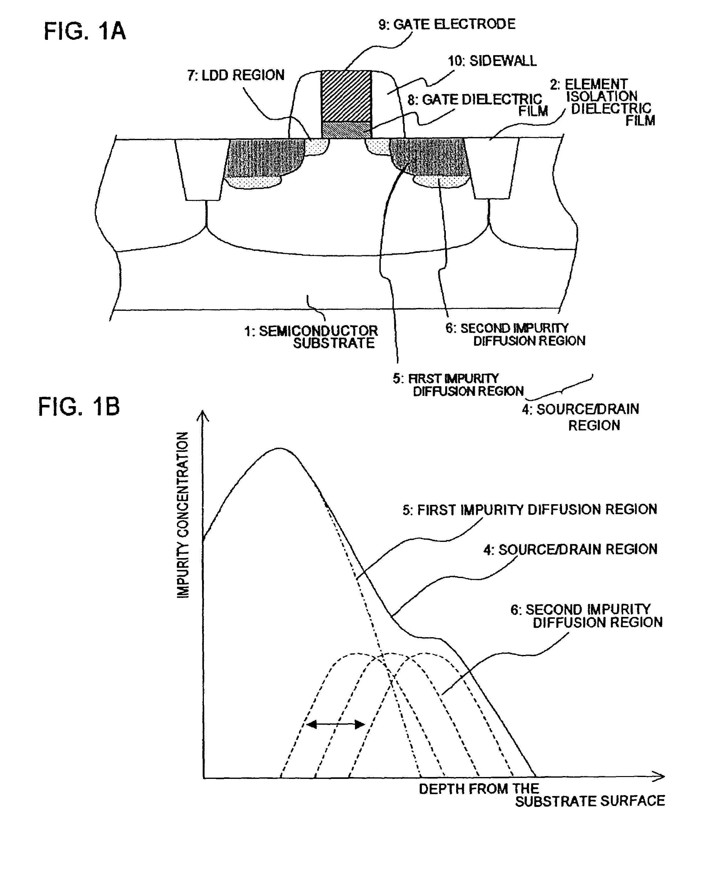
[0069]FIGS. 1A and 1B are schematic cross-sectional drawings showing a structure of a semiconductor device provided with a P-MOS transistor according to an example of the present invention.

[0070]Firstly, a structure of a semiconductor device according to this example will be described referring to FIG. 1A. The semiconductor device of this example is provided with a P-MOS transistor including a source / drain region 4 consisting of a first impurity diffusion region 5 formed with B or BF2 utilizing a gate electrode 9 and a sidewall 10 as a mask in a P-MOS forming region isolated by an element isolation dielectric film 2, and a second impurity diffusion region 6 formed with In at a bottom portion of the firs...


PUM


Abstract

A technology of restraining junction leakage in a semiconductor device is to be provided. There is provided a semiconductor device provided with a semiconductor substrate, a gate electrode 9 formed on the semiconductor substrate, and a source/drain region formed beside the gate electrode, wherein the source/drain region 4 comprises a first impurity diffusion region including a first P-type impurity and located in the proximity of a surface of the semiconductor substrate, and a second P-type impurity diffusion region located below the first impurity diffusion region and including a second P-type impurity having a smaller diffusion coefficient in the semiconductor substrate than the first P-type impurity.

Description

[0001]This application is based on Japanese patent application Nos. 2003-058099 and 2003-272796, the contents of which are incorporated hereinto by reference.FIELD OF THE INVENTION[0002]The present invention relates to a semiconductor device and a method of manufacturing the same.BACKGROUND OF THE INVENTION[0003]Along with the progressing micronization of semiconductor devices, there has arisen a problem that a leakage current increases while a transistor is off, because of a so called short channel effect caused by expansion of a depletion layer around a drain diffusion layer toward a channel. For restraining the short channel effect, up until now an LDD (Lightly Doped Drain) structure has popularly been utilized, whereby an offset gate layer having a lower impurity concentration is formed between a gate and a source or a drain so as to achieve an impurity concentration gradient, and in order to cope with a further micronization of semiconductor devices, a technique of forming a sh...

Claims


Application Information

Patent Timeline
IPC IPC(8): H01L29/167H01L21/265H01L21/336H01L21/8238H01L27/092H01L29/78
CPCH01L21/26513H01L21/823807H01L21/823814H01L29/6659H01L29/7833H01L21/823842Y10S257/917H01L21/2658
Inventor MASUOKA, YURIKIMIZUKA, NAOHIKO
Owner RENESAS ELECTRONICS CORP
Why Eureka
Try Eureka