Lithographic apparatus, device manufacturing method and substrate holder

a technology of lithographic apparatus and substrate, which is applied in the direction of electrical apparatus, printers, instruments, etc., can solve the problems of reducing yield and throughput, unable to clamp, and requiring the discarding of such substrates, so as to achieve the effect of more reliably clamping concave substrates

Active Publication Date: 2006-04-18
ASML NETHERLANDS BV
View PDF10 Cites 1 Cited by
  • Summary
  • Abstract
  • Description
  • Claims
  • Application Information

AI Technical Summary

Benefits of technology

[0011]One aspect of the present invention is to provide a substrate holder that can more reliably clamp concave substrates.
[0013]By reducing the height of the protrusions (which are also sometimes referred to as pimples or burls) and ensuring that a relatively large number of vacuum ports opens into a central region of the substrate holder, it is possible to ensure that a vacuum develops under the substrate even when the substrate is significantly concave. The pressure differential across the substrate tends to flatten the substrate enabling the initial vacuum to deepen, increasing the pressure differential and further flattening the substrate. It is therefore only necessary to develop an initial vacuum under the central region of the substrate to successfully clamp a substrate. The initial vacuum is sufficient to have a flattening effect on the substrate but need not be as deep as the vacuum developed when the substrate is clamped. The necessary depth of the initial vacuum will depend on the mechanical properties and curvature of the substrates to be clamped. Once the substrate has been clamped it is flattened against the tops of the protrusions and the clamping effect is the same as if the substrate had been flat in the first place.
[0014]It is preferred that the protrusions have a height of no less than 60 μm to ensure that the vacuum pressure under the substrate rapidly becomes uniform when the substrate is clamped. It is most preferred that the height of the protrusions is in the range of from 70 to 80 μm. With protrusions of such a height, the inventors have discovered that silicon substrates of standard dimensions with a curvature of up to 800 μm across a 300 mm wafer can be successfully clamped.

Problems solved by technology

The known designs of substrate holder suffer from the problem that if a concave (dished) substrate is placed on them it fails to be clamped because the wide gap between the raised edges of the substrate and the surrounding wall means that no vacuum develops underneath the substrate.
Substrates can become concave due to processes carried out on them to build devices and may be discarded if they become too dished to be clamped onto the substrate table.
The need to discard such substrates reduces yield and throughput.

Method used


Image

  • Lithographic apparatus, device manufacturing method and substrate holder
  • Lithographic apparatus, device manufacturing method and substrate holder
  • Lithographic apparatus, device manufacturing method and substrate holder

Examples


Embodiment Construction

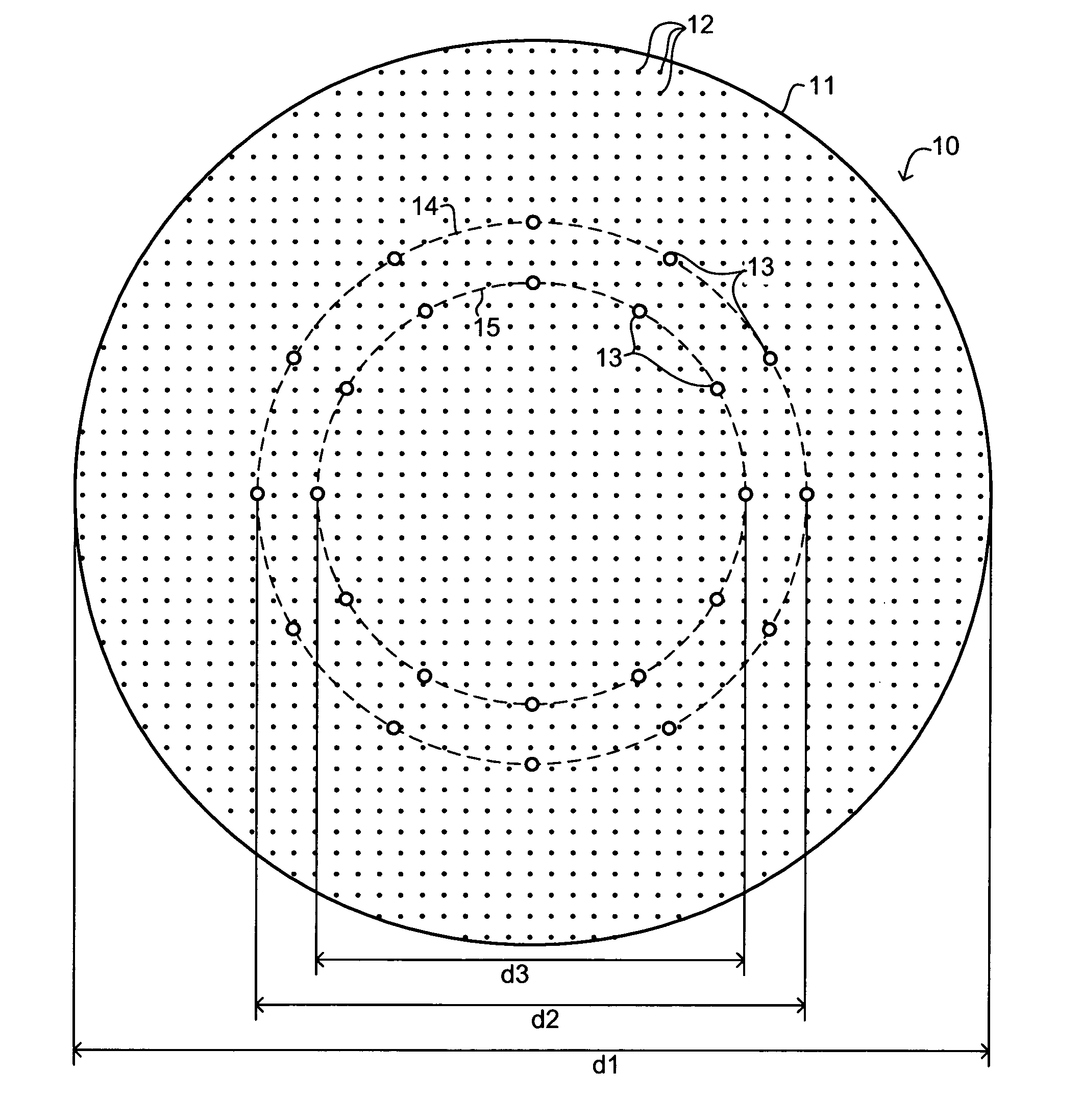
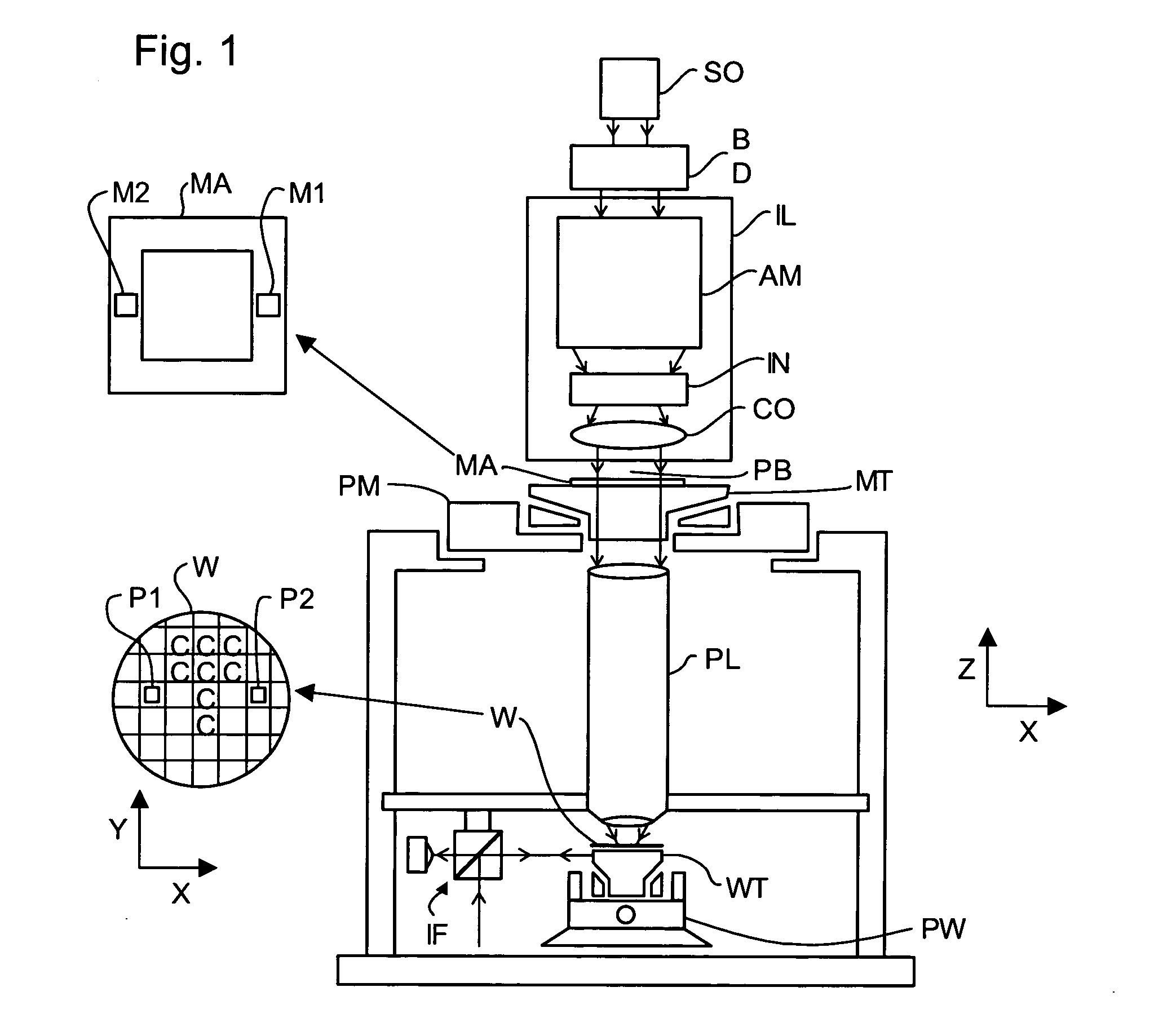
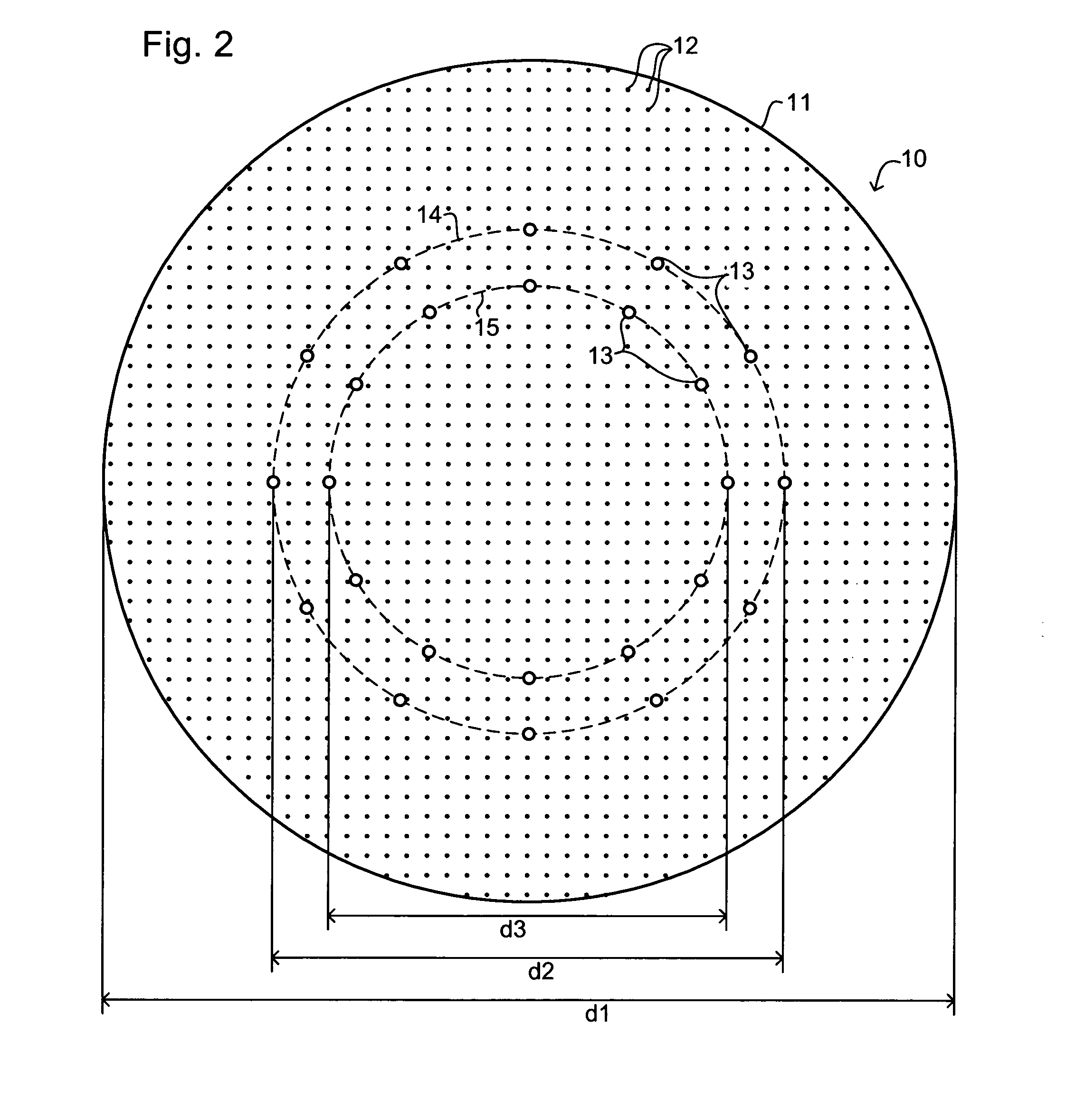
[0033]FIG. 1 schematically depicts a lithographic apparatus according to an embodiment of the invention. The apparatus comprises: an illumination system (illuminator) IL for providing a projection beam PB of radiation (e.g. UV radiation or DUV radiation), which in this particular case also comprises a radiation source SO; a first support structure (e.g. a mask table) MT for supporting patterning device (e.g. a mask) MA and connected to first positioning structure PM for accurately positioning the patterning device with respect to a projection system (“lens”) PL; a substrate table (e.g. a wafer table) WT for holding a substrate (e.g. a resist-coated wafer) W and connected to second positioning structure PW for accurately positioning the substrate with respect to the projection system PL; and the projection system (e.g. a refractive projection lens) PL for imaging a pattern imparted to the projection beam PB by patterning device MA onto a target portion C (e.g. comprising one or more ...


PUM

PropertyMeasurementUnit
heightaaaaaaaaaa
heightaaaaaaaaaa
heightaaaaaaaaaa

Abstract

A substrate holder has burls having a height not less than 100 μm and at least 10 vacuum ports arranged within a central region extending to a radius of two thirds the radius of the substrate. Thereby concave wafers can be reliably clamped by generating an initial vacuum in a central region which exerts a clamping force tending to flatten the wafer and allowing the initial vacuum to deepen until the wafer is fully clamped.

Description

[0001]The present application claims priority to European Application No. 02258833.9, filed on Dec. 20, 2002, the entirety of which is hereby incorporated into the present application by reference thereto.BACKGROUND OF THE INVENTION[0002]1. Field of the Invention[0003]The present invention relates to a lithographic apparatus, a method of manufacturing a device, and a substrate holder.[0004]2. Brief Description of Related Art[0005]A lithographic apparatus is a machine that applies a desired pattern onto a target portion of a substrate. Lithographic apparatus can be used, for example, in the manufacture of integrated circuits (ICs). In that circumstance, a patterning device, such as a mask, may be used to generate a circuit pattern corresponding to an individual layer of the IC, and this pattern can be imaged onto a target portion (e.g. comprising part of, one or several dies) on a substrate (e.g. a silicon wafer) that has a layer of radiation-sensitive material (resist). In general, ...

Claims


Application Information

Patent Timeline
Patent Type & Authority Patents(United States)
IPC IPC(8): G03B27/58G03B27/42H01L21/683G03F7/20H01L21/027
CPCG03F7/70783G03F7/707H01L21/027
Inventor VAN BALLEGOIJ, ROBERTUS NICODEMUS JACOBUSCUIJPERS, MARTINUS AGNES WILLEMMEIJERS, PIETER JOHANNES GERTRUDISVAN NUNEN, GERARDUS PETRUS MATTHIJSOTTENS, JOOST JEROEN
Owner ASML NETHERLANDS BV
Why Eureka
Try Eureka