Methods for magnetically establishing an electrical connection with a contact of a semiconductor device component

a technology of magnetic connection and semiconductor device, which is applied in the direction of coupling device connection, magnetic body, instruments, etc., can solve the problems of unreliable semiconductor device sold and used, failure of semiconductor device, damage to the wafer, etc., and achieve the effect of decreasing increasing the temperature of the semiconductor devi

Inactive Publication Date: 2006-04-25
MICRON TECH INC
View PDF26 Cites 46 Cited by
  • Summary
  • Abstract
  • Description
  • Claims
  • Application Information

AI Technical Summary

Problems solved by technology

For example, about 10 milliamps (mA) of current may be applied to each semiconductor device carried upon a substrate as the temperature of the semiconductor device is cycled between ambient temperature and a temperature of at least about 100° C. Such cycling of the temperature of the semiconductor device as current is being applied thereto is intended to stress the semiconductor device by driving any contaminants therein into the active circuitry thereof, thus causing failure of the semiconductor device.
This type of stress testing is known in the art to cause the early failure of unreliable semiconductor devices, thereby preventing these unreliable semiconductor devices from being sold and used.
As a result, a large amount of pressure may be applied to a small area on the wafer, which may cause damage to the wafer that may, in turn, damage semiconductor devices carried by the wafer.
In addition, as the temperature of the burn-in oven is increased, the alligator clips may expand and, thus, be moved along the wafer, which may also damage the wafer, as well as the semiconductor devices formed thereon.
While C-clamps contact larger areas of the respective common ground and power (VCC) contacts formed on the active surface of a wafer, as well as larger areas on the backside of the wafer, and apply force to the wafer in a direction substantially normal, or perpendicular, to the plane of the wafer, C-clamps are relatively clumsy and would, therefore, likely increase the chance that a wafer is damaged as C-clamps are secured to their respective contacts.
Moreover, when stress testing involves varied temperatures, the expansion of a C-clamp would increase the amount of force applied to the wafer, which could crack or otherwise damage the wafer, as well as semiconductor devices carried upon the wafer.
Conversely, contraction of a C-clamp during cooling could result in an inadequate electrical connection between the C-clamp and its corresponding contact.
Thus, the amount of power and voltage applied to each die during wafer-level burn-in testing may not be consistent or repeatable when alligator clips or C-clamps are used to supply a burn-in voltage to dice through a common contact on the wafer or other substrate.
No known apparatus or method for establishing an electrical contact with a common contact on a wafer is available which does not induce stress on or in the wafer.
No known apparatus or method in wafer-scale stress testing of semiconductor devices is available without applying too much force or too little force to the wafer.

Method used


Image

  • Methods for magnetically establishing an electrical connection with a contact of a semiconductor device component
  • Methods for magnetically establishing an electrical connection with a contact of a semiconductor device component
  • Methods for magnetically establishing an electrical connection with a contact of a semiconductor device component

Examples


Embodiment Construction

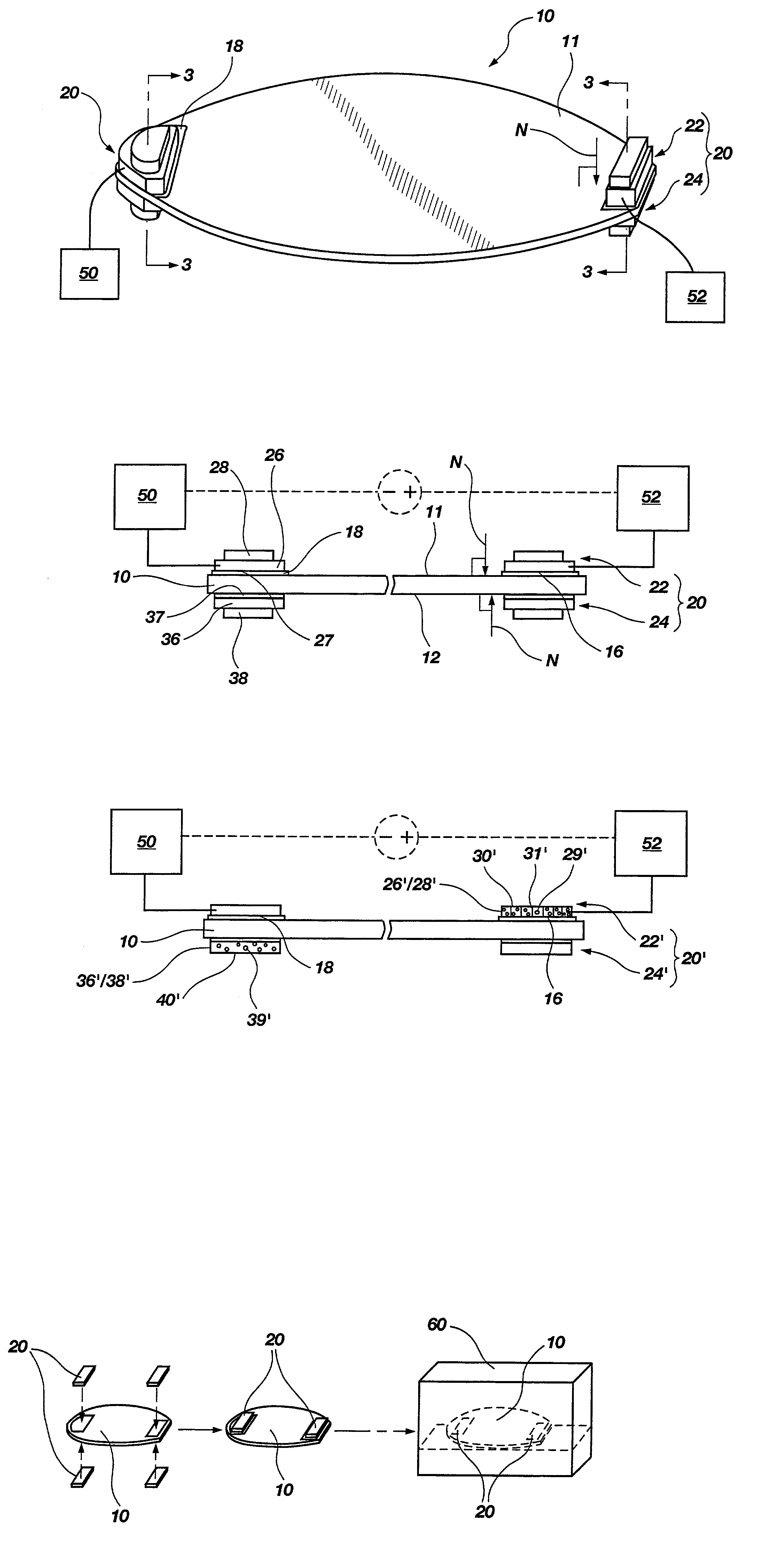
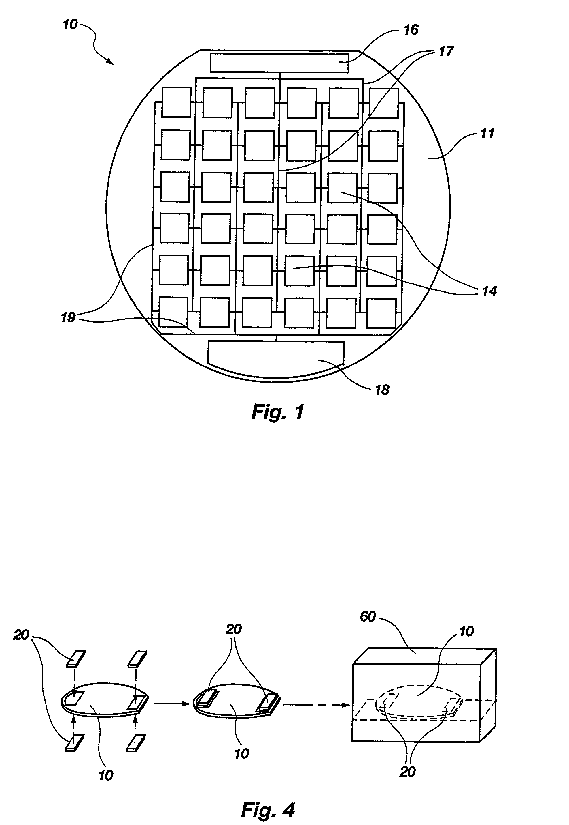
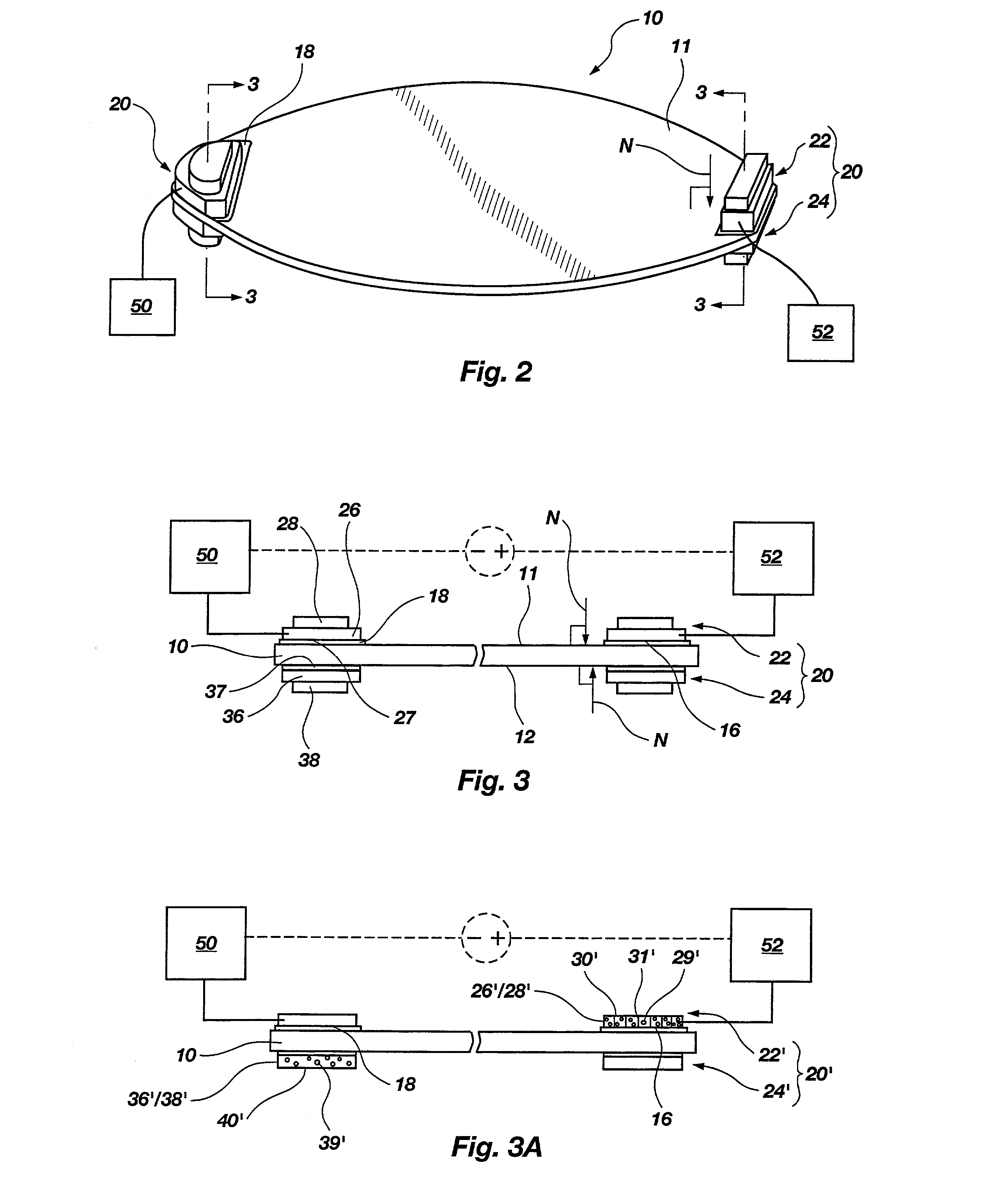
[0025]A semiconductor wafer, referred to herein as a substrate 10, which includes a plurality of semiconductor devices 14 carried upon an active surface 11 thereof, is illustrated in FIG. 1. Substrate 10 also includes, on active surface 11, a common ground contact 16 and a common power (VCC) contact 18. Common ground contact 16 and common power (VCC) contact 18 both communicate with a number of different semiconductor devices 14 on substrate 10 by way of respective circuit traces 17, 19 carried upon active surface 11 of substrate 10. Although substrate 10 is illustrated in FIG. 1 as a semiconductor wafer, the hereinafter described electrical connector of the present invention may be used with other substrates, including, without limitation, individual semiconductor dice, full or partial wafers formed of semiconductive material (e.g., silicon, gallium arsenide, iridium phosphide, etc.), and silicon-on-insulator (SOI) substrates, such as silicon-on-glass (SOG), silcon-on-sapphire (SOS...


PUM

PropertyMeasurementUnit
temperatureaaaaaaaaaa
currentaaaaaaaaaa
contact resistanceaaaaaaaaaa

Abstract

An electrical connector configured to nonrigidly apply force to a semiconductor substrate in directions substantially normal to a plane of the semiconductor substrate includes a first member with an electrically conductive element and a first attractive element and a second member that includes a support element and a second attractive element. Attractive forces, such as magnetic attraction, between the first and second attractive elements secure the first and second members of the electrical connector to the semiconductor substrate in a manner that facilitates communication between the electrically conductive element of the first member and one or more semiconductor devices carried upon the semiconductor substrate. The electrical connector may be used in stress testing of semiconductor devices or to otherwise establish an electrical connection between one or more semiconductor devices, a ground, and a power source.

Description

CROSS-REFERENCE TO RELATED APPLICATION[0001]This application is a continuation of application Ser. No. 09 / 777,986, filed Feb. 6, 2001, now U.S. Pat. No.6,340,302, issued Jan. 22, 2002.BACKGROUND OF THE INVENTION[0002]1. Field of the Invention[0003]The present invention relates to methods and apparatus for effecting wafer-level burn-in, or stress testing, of semiconductor devices and, more particularly, to apparatus and methods for establishing an electrical connection between semiconductor devices on a wafer or other substrate including multiple semiconductor devices thereon and burn-in test equipment. Specifically, the present invention relates to apparatus and methods that employ a magnetic field to establish an electrical connection between semiconductor devices carried upon a wafer or other substrate and burn-in test equipment.[0004]2. Background of the Related Art[0005]Once semiconductor devices have been fabricated, the semiconductor devices or representative samples thereof a...

Claims


Application Information

Patent Timeline
Patent Type & Authority Patents(United States)
IPC IPC(8): H01S4/00G01R1/04G01R31/28
CPCG01R1/0416G01R31/2863H01R13/6205G01R31/2831G01R31/3025H01R13/22Y10T29/49174Y10T29/49169Y10T29/49204Y10T29/49126Y10T29/49004Y10T29/4913H01R2201/20
Inventor LADD, JOHN W.
Owner MICRON TECH INC
Why Eureka
Try Eureka