Self light emitting display device

Active Publication Date: 2006-04-25
DAWNCREST IP LLC
View PDF2 Cites 42 Cited by
  • Summary
  • Abstract
  • Description
  • Claims
  • Application Information

AI Technical Summary

Benefits of technology

[0012]The present invention has been made in view of the above circumstances. An object of the present invention is to provide a techn

Problems solved by technology

Therefore, there is a limitation with respect to a display device for mobile telephone use, for which a reduction in thickness is required.
However, there is the following problem with respect to the double-sided display de

Method used


Image

  • Self light emitting display device
  • Self light emitting display device
  • Self light emitting display device

Examples


Example

(Embodiment 1)

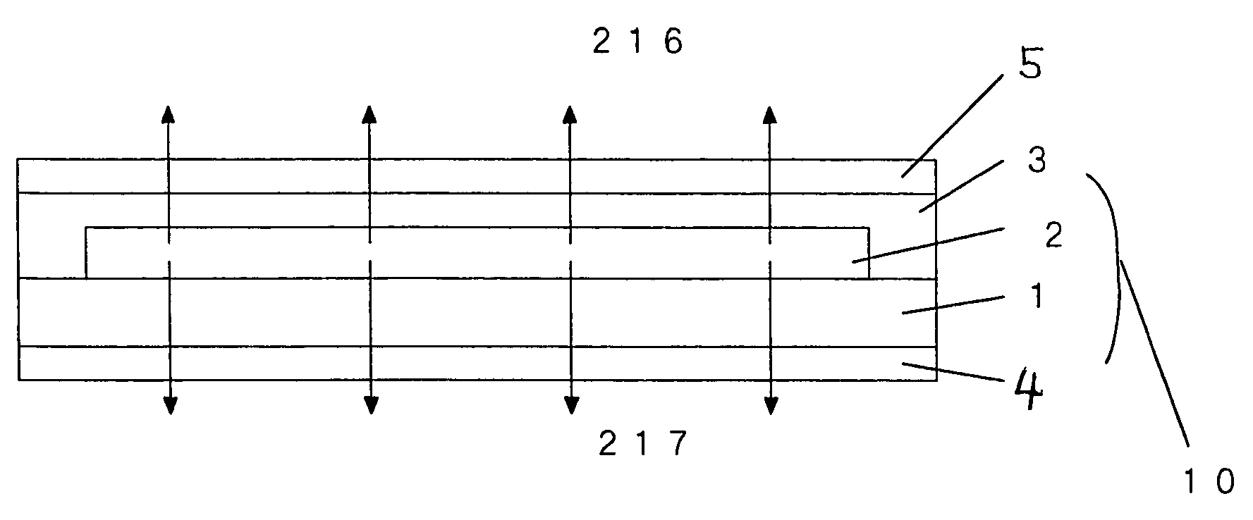
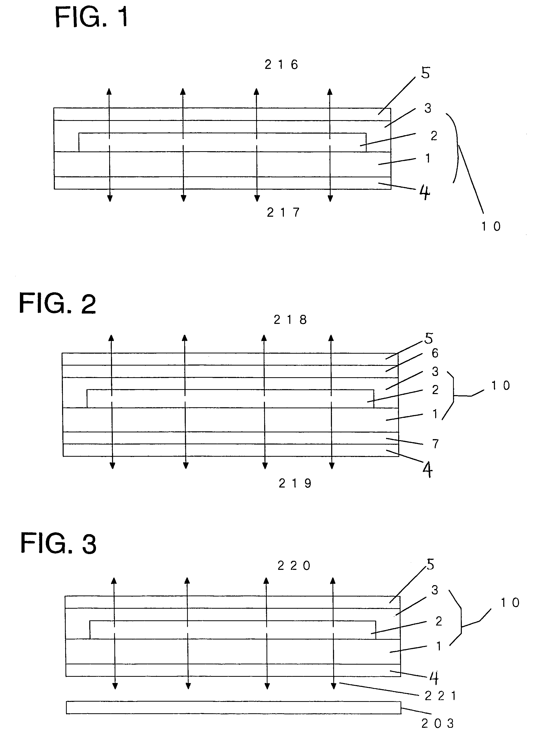
[0041]FIG. 1 is a schematic sectional view showing an organic EL device of this embodiment. As shown in FIG. 1, an organic EL element portion 2 is formed on the surface of a substrate 1. The organic EL element portion 2 is sealed with a sealing structure 3, thereby composing an organic EL cell 10. A first polarization layer 4 and a second polarization layer 5 are disposed at both ends of the organic EL cell such that transmission axes thereof are orthogonal to each other.

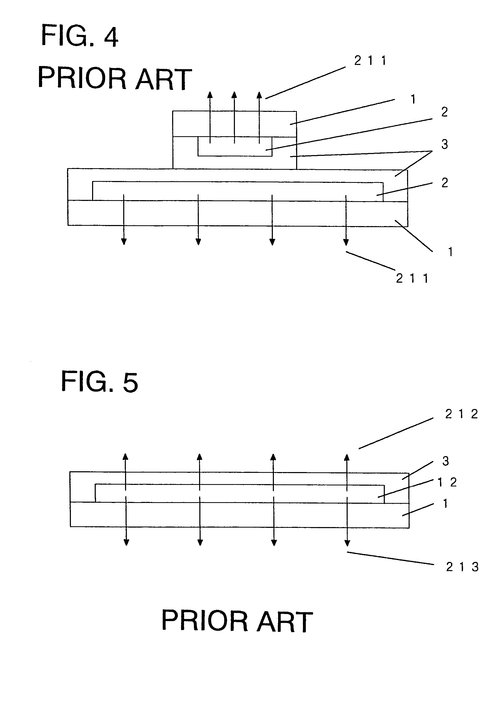
[0042]A display principle of an organic EL device having such a structure will be described with reference to FIG. 10. The first polarization layer 4 and the second polarization layer 5 are disposed at both sides of the organic EL cell 10. A transmission axis L7 of the first polarization layer 4 is orthogonal to a transmission axis L6 of the second polarization layer 5. EL light 121 emitted from a light emitting portion 101 of the organic EL cell 10 transmits through the second polarization layer 5 hav...

Example

(Embodiment 2)

[0049]FIG. 2 is a schematic view showing a sectional structure of an organic EL device according to Embodiment 2. Note that the description of the organic EL cell 10 overlapped with Embodiment 1 is omitted here as appropriate. As shown in FIG. 2, the organic EL device includes a first polarization layer 4 and a second polarization layer 5 which sandwich therebetween the organic EL cell 10; a first optical phase differential layer 7 (retardation: Än1d1, where Än is optical anisotropy and d is a thickness) provided between the organic EL cell 10 and the first polarization layer 4; and a second optical phase differential layer 6 (retardation: Än2d2) provided between the organic EL cell 10 and the second polarization layer 5. A transmission axis of the first polarization layer 4 is parallel to a transmission axis of the second polarization layer 5, a delay phase axis of the optical anisotropy of the first optical phase differential layer 7 (Än1d1) is parallel to a delay ph...

Example

(Embodiment 3)

[0057]FIG. 3 is a schematic sectional view of an organic EL device of this embodiment. Note that the descriptions overlapped with above-mentioned respective embodiments are omitted here as appropriate. As shown in FIG. 3, the first polarization layer 4 and the second polarization layer 5 are disposed in both sides of the organic EL cell 10 such that transmission axes thereof are orthogonal to each other. In this embodiment, a polarizing plate is used for the polarization layers. Further, a privacy device in the form of a shutter 203 is located outside the first polarization layer 4 so as to correspond to a light emitting region of the organic EL cell 10. The case where the organic EL device shown in FIG. 3 is applied to a foldable information device having two foldable connected sections as shown in FIGS. 12 and 13 will be described as an example. In a state in which the information device is folded and the two sections overlap (FIG. 12), the shutter 203 is opened. The...


PUM


Abstract

Provided is a technique for producing a double-sided display device using a self light emitting display element in which a thickness thereof is small, a contrast is high, and a privacy is kept. A first polarization layer and a second polarization layer are provided so as to sandwich the self light emitting display element and it is set such that the transmission axis of the first polarization layer and the transmission axis of the second polarization layer are orthogonal to each other.

Description

BACKGROUND OF THE INVENTION[0001]The present invention relates to a display device using a light emitting element of a self light emission type, such as an EL (electroluminescence) element that emits light by application of a voltage.[0002]An EL element is a light emitting element having a great potential because light emission is produced at a relatively low voltage and manufacturing thereof is easy. An element life, which has been a problem in a practical use of the EL element, now reaches a practical level. Accordingly, the EL element is beginning to be adopted for an in-car audio system and a mobile telephone.[0003]FIG. 6 shows a structure of a conventional EL element. As shown in FIG. 6, in the EL element, a transparent electrode 31 made of indium tin oxide (ITO) or the like, a hole transporting layer 32, a light emitting layer 33, and an electrode 34 made of aluminum or the like are laminated in succession on a substrate 1 made of glass or the like. Here, an EL element portion...

Claims


Application Information

Patent Timeline
IPC IPC(8): H05B33/00G02F1/13G02F1/00G02F1/03G02F1/13363G09F9/30H01L27/32H01L51/50H01L51/52H05B33/02H05B33/14H05B33/22
CPCH01L51/5281H01L2251/5323H10K50/86H10K2102/3031H05B33/22
Inventor SENBONMATSU, SHIGERU
Owner DAWNCREST IP LLC
Why Eureka
Try Eureka