Low leakage SRAM scheme

a low leakage and leakage current technology, applied in the field of memory devices, can solve the problems of inability to reduce leakage, significant periphery leakage, and total chip current leakage using this approach

Active Publication Date: 2006-05-02
TEXAS INSTR INC
View PDF7 Cites 31 Cited by
  • Summary
  • Abstract
  • Description
  • Claims
  • Application Information

AI Technical Summary

Problems solved by technology

With the continued increment in the transistor leakage and the number of transistors on a chip, however, the total chip current leakage using this approach has become completely unacceptable for wireless applications based on state of art semiconductor technologies.
The problem with the above approach is that the periphery leakage becomes significant as compared with the array leakage that is aggressively reduced by using much reduced voltages across the array and other advanced techniques, such as disclosed in the commonly assigned cross referenced patent application, the teaching of which is incorporated herein by reference.
Even with the use of longer gate length or higher nwell bias, etc., the periphery current leakage cannot be reduced to significantly below the level of the array leakage in advanced CMOS technologies, since the direct gate tunneling leakage cannot be reduced.
The problem with this approach is that the transition of control of the word lines between the periphery circuit word line drivers to the low power mode circuits is critical, and particularly difficult because of the relatively large word line drivers.
Further, the circuitry required to hold each word line off may incur significant leakage.

Method used


Image

  • Low leakage SRAM scheme
  • Low leakage SRAM scheme
  • Low leakage SRAM scheme

Examples


first embodiment

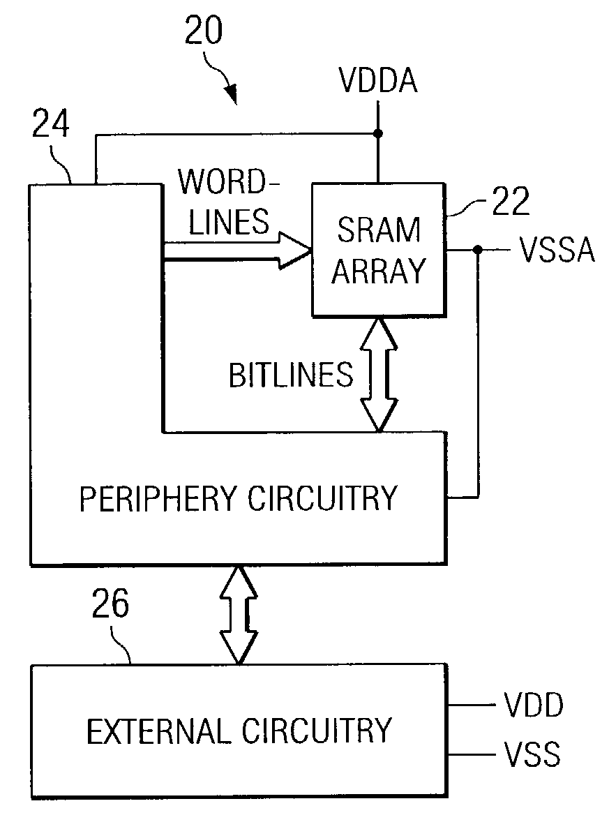
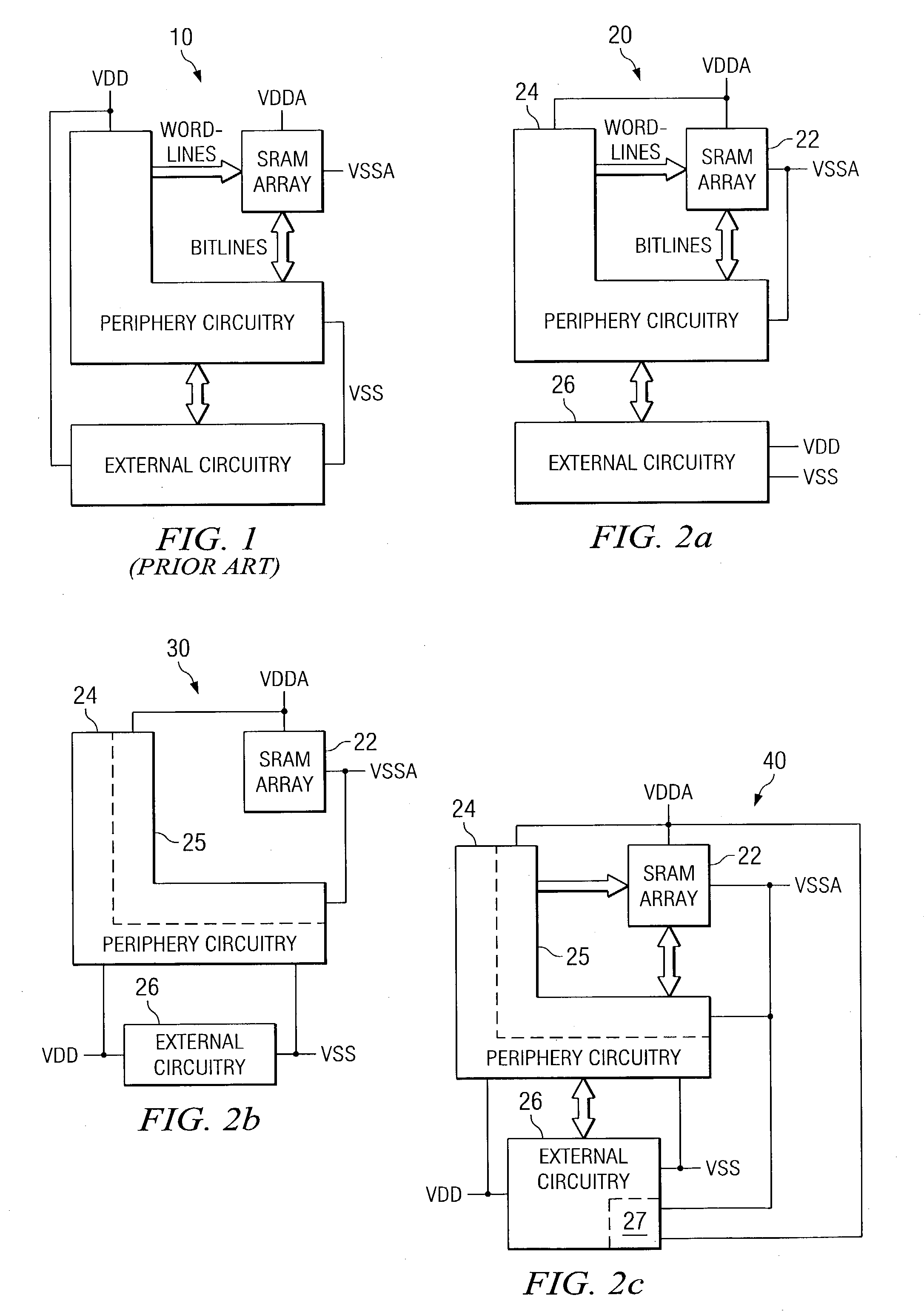
[0021]In the first embodiment shown at 20 in FIG. 2a the full memory periphery circuitry 24 is powered with the memory array 22 supplies, VDDA and / or VSSA. Memory control signals in the periphery circuitry 24 are set to have the memory array 22 unaccessed, such that the powered row periphery circuitry maintains all word lines off. Further, the memory control signals are set to have the column periphery circuitry output drivers in tri-state, so that the powered column periphery circuitry does not drive the external circuitry 26 data lines. For transition into the power down mode, the preferred sequence is to first set the control signals in the periphery circuitry 24, followed by transitioning VDDA and / or VSSA to the power down levels and reducing and / or removing power to selected external circuitry 26. For transition from the power down mode to the active mode, the preferred sequence is to restore VDDA and / or VSSA to the active levels and to restore active power to the selected exte...

second embodiment

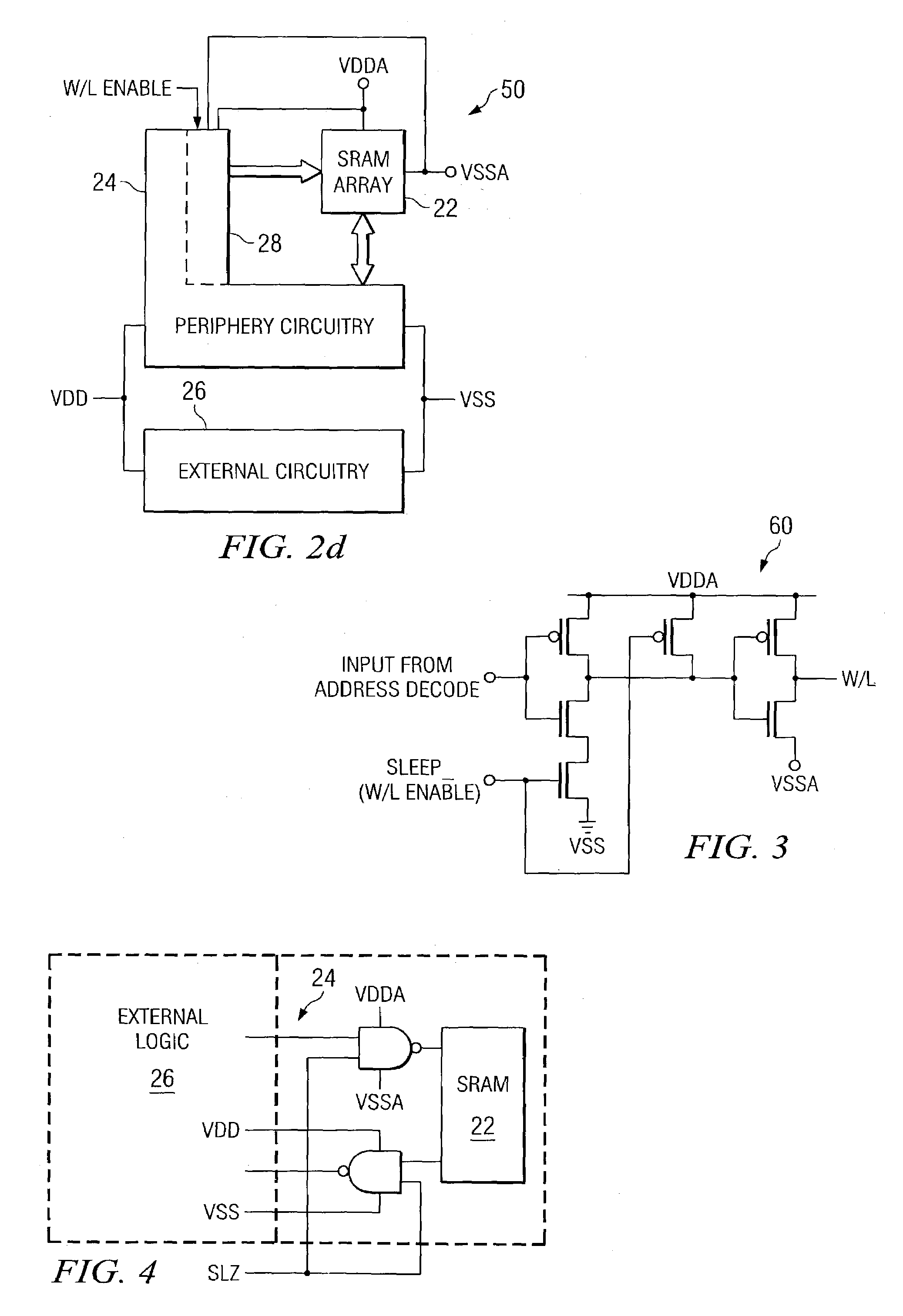
[0022]In the second embodiment shown at 30 in FIG. 2b, the word line drivers in the portion 25 of periphery circuitry 24 are powered with the array supplies VDDA and / or VSSA, and other periphery circuits outside of portion 25 are powered similar to external circuitry 26. Circuits are provided, such as illustrated at 60 in FIG. 3, to ensure that the input to the word line drivers during the power down mode is such to keep the word lines off. It is efficient to have circuitry with the dual function of selectively enabling word lines in the active mode and ensuring the word lines are off in the power down mode. The word line enable circuitry may be immediately before the word line drivers, as in FIG. 3, or there may be additional circuits, such as a buffering inverters, between the word line enable circuits and the word line drivers. The portion 25 of periphery circuitry 24 may include all circuits from the word line enable circuits to and including the word line drivers. For transitio...

third embodiment

[0023]In the third embodiment shown at 40 in FIG. 2c a portion 27 of the external circuitry is supplied with VDDA and / or VSSA.


PUM


Abstract

A memory device (20) having substantially reduced leakage current in a sleep / data retention mode whereby at least a portion (25, 28) of the periphery circuitry (24) shares the same power supplies VDDA and / or VSSA of the memory array (22) such that during sleep / data retention mode the voltage across both the portion (25, 28) of the periphery circuitry (24) and the memory array (22) of the selected SRAM block is reduced, while all other circuits can be shut down except the sleep control circuits as well as selected latches, flip-flops, etc. whose contents need to be retained. A sequence for powering up and shutting down portions of the periphery circuitry (24) and the external circuitry (26) is also provided.

Description

CROSS REFERENCE TO RELATED APPLICATIONS[0001]Cross reference is made to commonly assigned patent application Ser. No. 10 / 337,069 entitled “BIT-LINE CONTROL FOR LOW POWER IN STANDBY” filed Jan. 6, 2003, the teachings of which are incorporated herein by reference.FIELD OF THE INVENTION[0002]The present invention is generally related to memory devices, and more particularly to memory cells and leakage current thereof in a sleep / data retention mode.BACKGROUND OF THE INVENTION[0003]Circuits comprising or associated with a memory include the memory cell array that stores the data, memory periphery circuits that enable access to the memory cell array for READ and for WRITE, and external circuits. The memory cell array is generally arranged in rows and columns. Word lines that control access to the cells run in the row direction. Bit lines that carry data to and from the cell run in the column direction. The memory periphery circuits comprise row periphery that drives the word lines, column...

Claims


Application Information

Patent Timeline
Patent Type & Authority Patents(United States)
IPC IPC(8): G06F1/32G06F1/30G11C5/14G11C7/12G11C7/22
CPCG11C5/14G11C7/22G11C7/12G11C2207/2227
Inventor DENG, XIAOWEIHOUSTON, THEODORE W.
Owner TEXAS INSTR INC
Why Eureka
Try Eureka