
Method of fabricating flip chip ball grid array package

a grid array and flip chip technology, applied in the direction of electrical equipment, semiconductor devices, semiconductor/solid-state device details, etc., can solve the problem of thicker packaging structure after singulation, and achieve the effect of reducing the thickness of the packaging structur

Active Publication Date: 2006-05-09
ADVANCED SEMICON ENG INC
View PDF5 Cites 9 Cited by
  • Summary
  • Abstract
  • Description
  • Claims
  • Application Information

AI Technical Summary

Benefits of technology

The present invention is about a method of making a flip chip ball grid array (FC-BGA) package for reducing the thickness of the packaging structure. The method involves adhering flip chips in cavities of a substrate, filling the cavities with an underfill, and connecting solder balls to the substrate. The substrate is then divided to separate the portion adhering to the flip chips. A sealing glue material is used to cover the flip chips. The substrate core layer is removed to reduce the thickness of the package. The technical effect of this invention is to reduce the thickness of the FC-BGA package structure while maintaining its structural strength.

Problems solved by technology

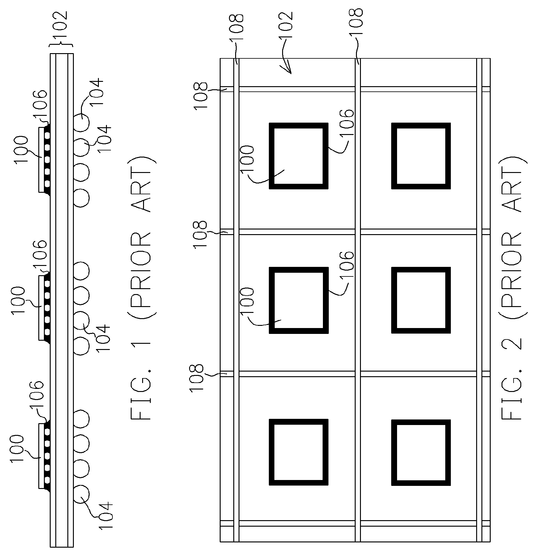
It is noted that, the conventional package method described above has the disadvantages that the packaging structure after singulation has a thicker thickness due to the substrate includes a core layer.

Method used


Image

  • Method of fabricating flip chip ball grid array package
  • Method of fabricating flip chip ball grid array package
  • Method of fabricating flip chip ball grid array package

Examples


Embodiment Construction

[0026]The present invention now will be described more fully hereinafter with reference to the accompanying drawings, in which preferred embodiments of the invention are shown. This invention may, however, be embodied in many different forms and should not be construed as limited to the embodiments set forth herein; rather, these embodiments are provided so that this disclosure will be thorough and complete, and will fully convey the scope of the invention to those skilled in the art. Like numbers refer to like elements throughout.

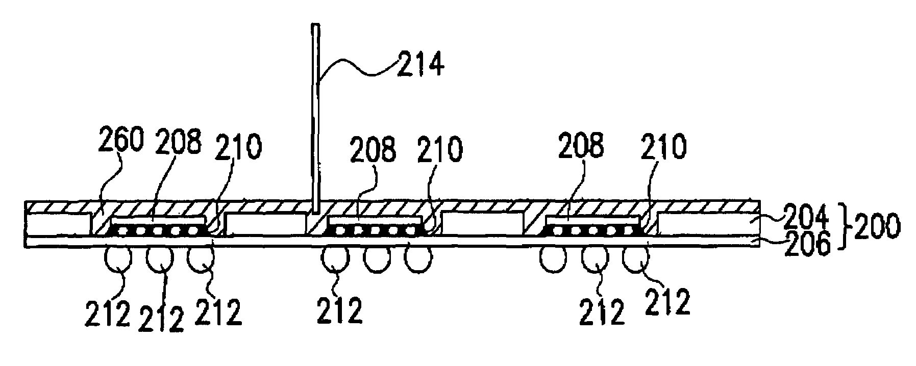
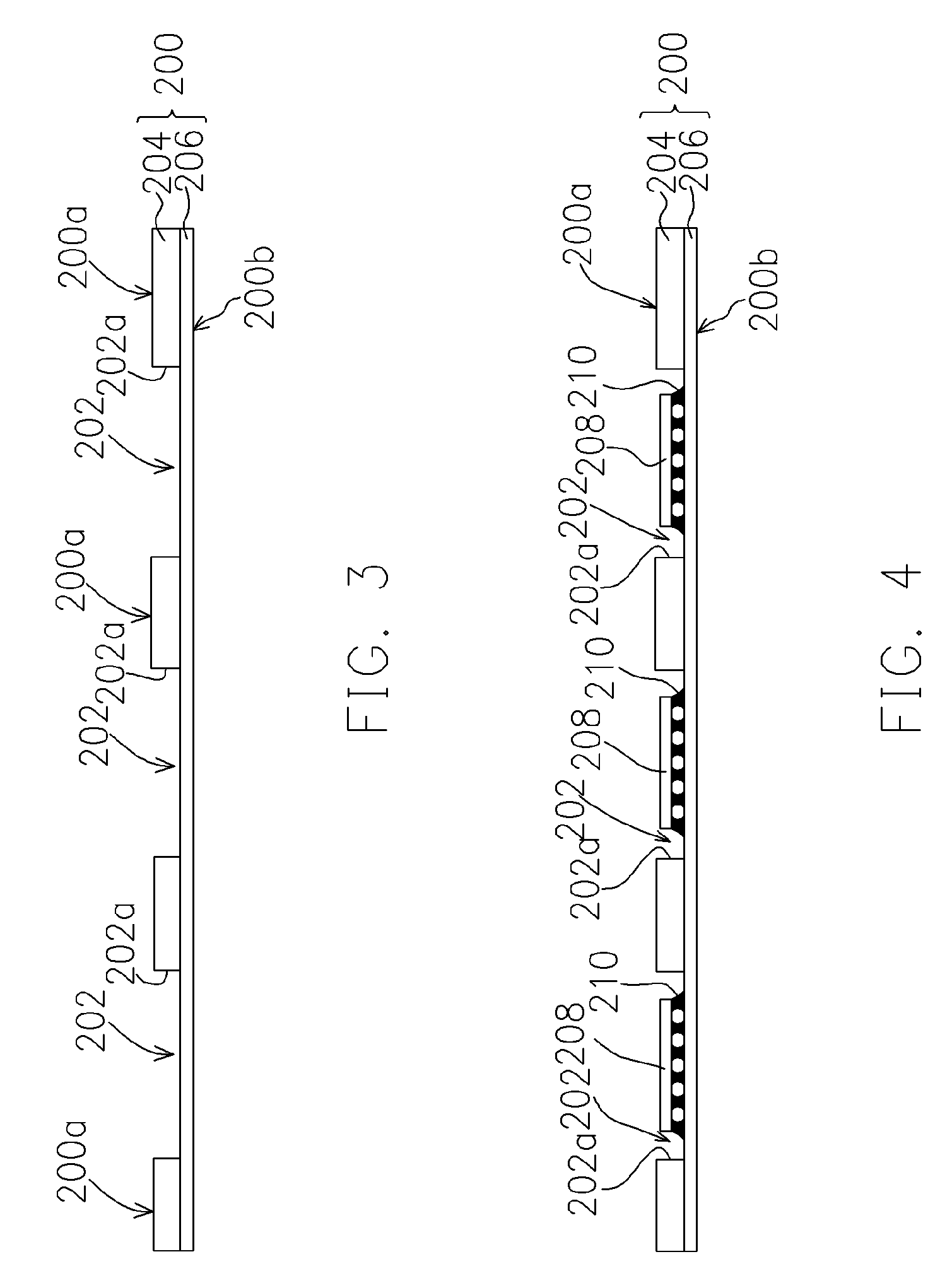
[0027]FIG. 3 to FIG. 6 are side cross-sectional views illustrating progressive steps of a method of fabricating a flip chip ball grid array (FC-BGA) package according to one embodiment of the present invention. Referring to FIG. 3, first, a substrate 200 including a first surface 200a and a second surface 200b is provided, wherein the first surface 200a includes a plurality of cavities 202. The reference number 202a represents a sidewall of the cavity 202....


PUM


Abstract

A method of fabricating a flip chip ball grid array (FC-BGA) package is provided. First, a substrate including a first surface and a second surface is provided, wherein the first surface includes a plurality of cavities. Then, a plurality of flip chips is adhered in the cavities of the substrate. Thereafter, an underfill filling step is performed to fill an underfill between the substrate the flip chips. Then, a ball placement step is performed to attach a plurality of solder balls to a second surface of the substrate. Thereafter, the substrate is divided to separate a portion of the substrate adhering to the flip chips from a sidewall of the cavities.

Description

CROSS REFERENCE TO RELATED APPLICATIONS[0001]This application claims the priority benefit of Taiwan application serial no. 92119938, filed Jul. 22, 2003.BACKGROUND OF INVENTION[0002]1. Field of the Invention[0003]The present invention relates to a method of fabricating a flip chip ball grid array (FC-BGA) package. More particularly, the present invention relates to a method of fabricating a slim flip chip ball grid array (FC-BGA) package.[0004]2. Description of Related Art[0005]Conventionally, a ball grid array (BGA) package structure generally includes chip, substrate and solder balls. The chip is electrically connected to the solder ball via the substrate, wherein the solder ball is provided for external connection. In other words, input / output contacts (binding pads) with a narrower interval inside the chip may be electrically connected to the solder balls with a wider interval via a circuit of the substrate (e.g., a printed circuit board, PCB). Therefore, the solder balls are us...

Claims


Application Information

Patent Timeline
Patent Type & Authority Patents(United States)
IPC IPC(8): H01L21/44H01L21/56H01L23/28H01L23/31
CPCH01L21/56H01L23/3128H01L24/97H01L21/563H01L2924/01033H01L2224/16H01L2224/73203H01L2224/97H01L2924/01029H01L2924/15311H01L2224/81
Inventor WANG, MENG-JEN
Owner ADVANCED SEMICON ENG INC
Learn More