Patch antenna having a non-feeding element formed on a side surface of a dielectric

a dielectric and side surface technology, applied in the field of digital radio receivers, can solve the problems of large interference of radiation elements, unsuitable antennas of planer-type (plane-type) such as patch antennas, and difficult to gain the directivity of the antenna in the low elevation mor

Inactive Publication Date: 2006-05-09
MITSUMI ELECTRIC CO LTD
View PDF12 Cites 18 Cited by
  • Summary
  • Abstract
  • Description
  • Claims
  • Application Information

AI Technical Summary

Benefits of technology

[0012]It is therefore an object of the present invention to provide a patch antenna which is capable of ensuring a directivity of an antenna in a low angle of elevation.
[0013]It is another object of the present invention to provide a patch antenna unit which is capable of reducing interference for a radiation element.
[0014]It is still another object of the present invention to provide a patch antenna which is capable of easily adjusting an antenna characteristic in the low angle of elevation.

Problems solved by technology

In general, it is understood that antennas of planer-type (plane-type) such as patch antennas are unsuited for the antenna for use in the digital radio receiver because the antennas of planer-type (plane-type) has a narrow directivity.
However, when only the ground plate is provided, it is difficult to gain the directivity of the antenna in the low angle of elevation more.
It is possible to improve an antenna characteristic in the microstrip antenna described in JP 11-284429 A. However, structure where the non-feeding elements are mounted on the top surface has large interference for a radiation element.
In addition, inasmuch as it is impossible to adjust the non-feeding elements up and down, it is happened in a case where it is impossible to satisfy a desired antenna characteristic.

Method used


Image

  • Patch antenna having a non-feeding element formed on a side surface of a dielectric
  • Patch antenna having a non-feeding element formed on a side surface of a dielectric
  • Patch antenna having a non-feeding element formed on a side surface of a dielectric

Examples


Embodiment Construction

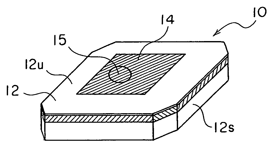
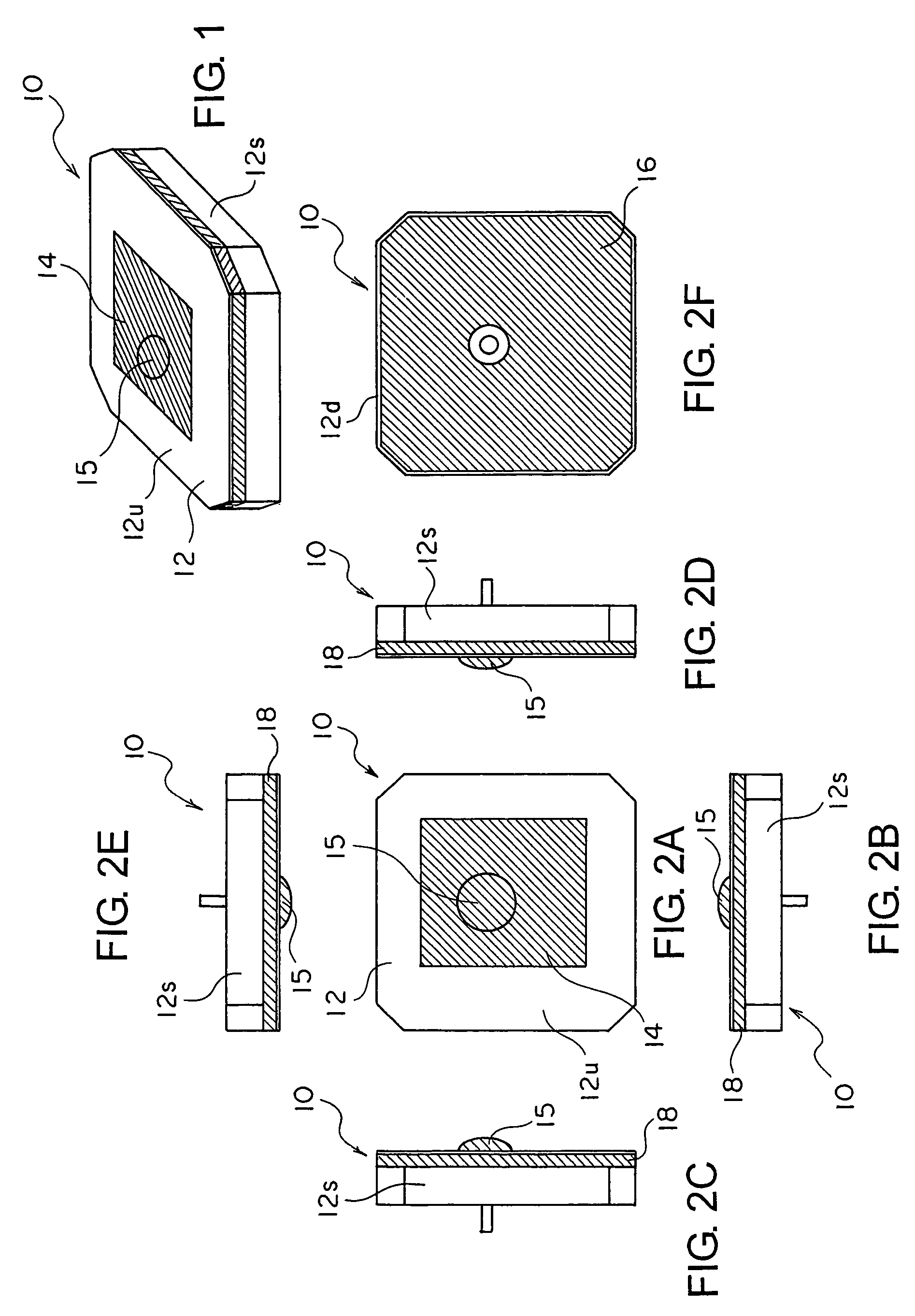
[0027]Referring to FIG. 1 and FIGS. 2A, 2B, 2C, 2D, 2E, and 2F, the description will proceed to a patch antenna 10 according to an embodiment of the present invention. FIG. 1 is a perspective view of the patch antenna 10. FIG. 2A is a plan view of the patch antenna 10. FIG. 2B is a front view of the patch antenna 10. FIG. 2C is a left-hand side view of the patch antenna 10. FIG. 2D is a right-hand side view of the patch antenna 10. FIG. 2E is a rear view of the patch antenna 10. FIG. 2F is a bottom view of the patch antenna 10.

[0028]The patch antenna 10 comprises a dielectric 12 having configuration of a substantially rectangular parallelepiped. In the example being illustrated, the dielectric 12 has a length, a width, and a thickness which are equal to 20 mm, 20 mm, and 4 mm, respectively. The dielectric 12 is made of a ceramic material or resin. The dielectric 12 has a top or upper surface 12u, a bottom surface 12d, and a side surface 12s. Practically, in the manner which is illus...


PUM


Abstract

In a patch antenna including a dielectric having a top surface, a bottom surface, and a side surface, a radiation element formed on the top surface of the dielectric, and a ground conductor formed on the bottom surface of the dielectric, a ring-shaped non-feeding element is formed on the side surface of the dielectric. The non-feeding element preferably may be formed on the side surface of the dielectric in the vicinity of the top surface of the dielectric. In addition, the non-feeding element may be formed by pasting a copper tape or by thick film printing.

Description

[0001]This application claims priority to prior Japanese patent application JP 2003-374222, the disclosure of which is incorporated herein by reference.BACKGROUND OF THE INVENTION[0002]This invention relates to a digital radio receiver for receiving an electric wave from an artificial satellite (that may be called a “satellite wave”) or an electric wave on the ground (that may be called a “terrestrial wave”) to listen in a digital radio broadcasting and, in particular, to a patch antenna for use in the digital radio receiver.[0003]In recent years, a digital radio receiver, which receives the satellite wave or the terrestrial wave to listen the digital radio broadcasting, has been developed and is put to practical use in the United State of America. The digital radio receiver is mounted on a mobile station such as an automobile and can receive an electric wave having a frequency of about 2.3 gigahertz (GHz) to listen in a radio broadcasting. That is, the digital radio receiver is a r...

Claims


Application Information

Patent Timeline
Patent Type & Authority Patents(United States)
IPC IPC(8): H01Q1/38H01Q7/00H01Q9/04H01Q13/08H01Q21/29
CPCH01Q1/38H01Q21/29H01Q9/0407H01Q7/00
Inventor NORO, JUNICHIAIZAWA, TOSHIAKI
Owner MITSUMI ELECTRIC CO LTD
Why Eureka
Try Eureka