Method for integrating high-k dielectrics in transistor devices

a technology of high-k dielectrics and transistors, applied in the field of semiconductor devices, can solve the problems of large gate tunneling leakage currents, limited ability to form thin oxide films with uniform thickness, and electrical and physical limitations to reduce the thickness of siosub>2 /sub>gate dielectrics, so as to facilitate semiconductor fabrication and mitigate defects in high-k dielectric layers. , the effect of reducing the risk of contamination

Active Publication Date: 2006-05-16
TEXAS INSTR INC
View PDF9 Cites 42 Cited by
  • Summary
  • Abstract
  • Description
  • Claims
  • Application Information

AI Technical Summary

Benefits of technology

[0010]The present invention provides systems and methods that facilitate semiconductor fabrication by integrating high-k dielectric layers into a process flow. The invention removes portions of deposited high-k dielectric layers not below gates and covers exposed portions (e.g., sidewalls) of high-k dielectric layers during fabrication with an encapsulation layer, which mitigates defects in the high-k dielectric layers and contamination of process tools. The encapsulation layer can also be employed as an etch stop layer and, at least partially, in comprising sidewall spacers.
[0011]A device of the present invention is fabricated by forming a high-k dielectric layer over a semiconductor substrate. An electrode material, such as polysilicon, is then formed on the high-k dielectric layer. The electrode material and the dielectric layer are then patterned, in separate patterning processes in one example, to form gate structures. The exposed high-k at the sidewall is encapsulated. Subsequently, extension regions are formed. In contrast, conventional devices typically form extension regions without patterning the dielectric layer. Other processing, including sidewall spacer formation and source / drain implants, are also performed. As a result, a semiconductor device can be fabricated with a substantially uniform equivalent oxide thickness.

Problems solved by technology

However, there are electrical and physical limitations on the extent to which thickness of SiO2 gate dielectrics can be reduced.
For example, very thin SiO2 gate dielectrics are prone to large gate tunneling leakage currents resulting from direct tunneling through the thin gate oxide.
In addition, there are conventional limitations on the ability to form such thin oxide films with uniform thickness.
Furthermore, thin SiO2 gate dielectric layers provide a poor diffusion barrier to dopants, for example, and may allow high boron dopant penetration into the underlying channel region of the silicon during device fabrication.
While the macroscopic composition (e.g., stoichiometry) of these materials may be controlled to a certain extent during such deposition processes, stoichiometric composition variations within the film may degrade device performance.
In addition, the above deposition techniques often create high-k dielectric films having defects that affect transistor performance.
Such defects may include oxygen vacancies, and / or other point defects affecting leakage through the gate dielectric.
Furthermore, certain deposition processes (e.g., CVD, ALD, etc.) may introduce impurities (e.g., C, OH, H, etc.) into the deposited high-k dielectric film, which also degrade device performance.
Moreover, the deposited film may not be of optimal density, wherein sub par performance may result in absent atomic rearrangement or realignment.
The integration of high-k films into the CMOS fabrication flow poses significant challenges.
The presence of a new metallic element on the wafer surface at an early stage of the device fabrication flow, as it is the case when high-k films are used as the gate dielectric of a CMOS device, poses a significant threat of cross contamination for the FEOL processes and tools.
In particular, wet treatments and thermal processes can be jeopardized by metallic contamination.

Method used


Image

  • Method for integrating high-k dielectrics in transistor devices
  • Method for integrating high-k dielectrics in transistor devices
  • Method for integrating high-k dielectrics in transistor devices

Examples


Embodiment Construction

[0026]One or more implementations of the present invention will now be described with reference to the attached drawings, wherein like reference numerals are used to refer to like elements throughout, and wherein the devices and structures illustrated in the figures are not necessarily drawn to scale.

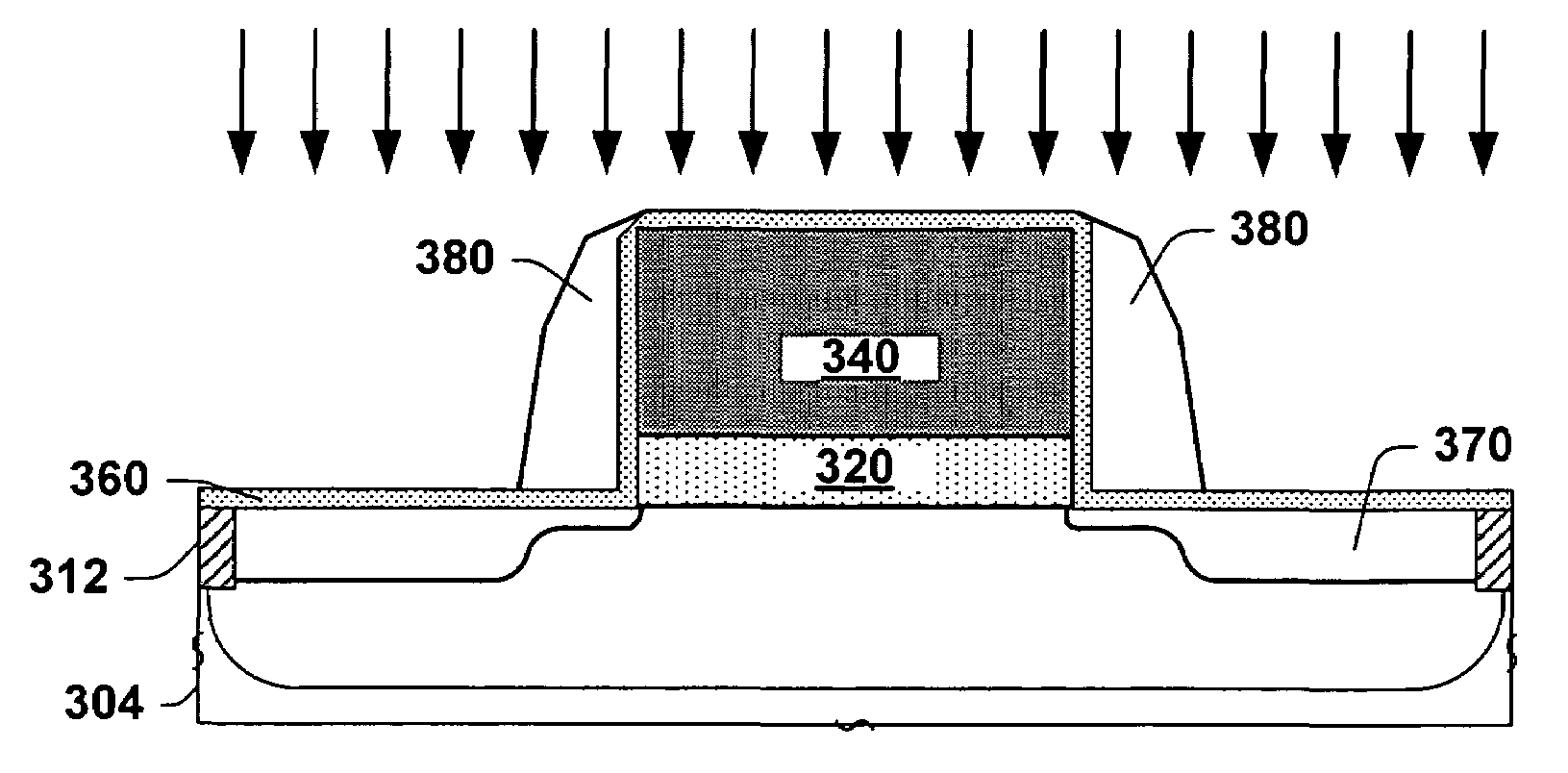
[0027]The present invention provides systems and methods that facilitate semiconductor fabrication by integrating high-k dielectric layers into a process flow. The invention removes portions of deposited high-k dielectric layers not below gates (e.g., source / drain regions) and covers exposed portions (e.g., sidewalls) of high-k dielectric layers during fabrication with an encapsulation layer, which mitigates defects in the high-k dielectric layers and contamination of process tools. The encapsulation layer can also be employed as an etch stop layer and, at least partially, in comprising sidewall spacers.

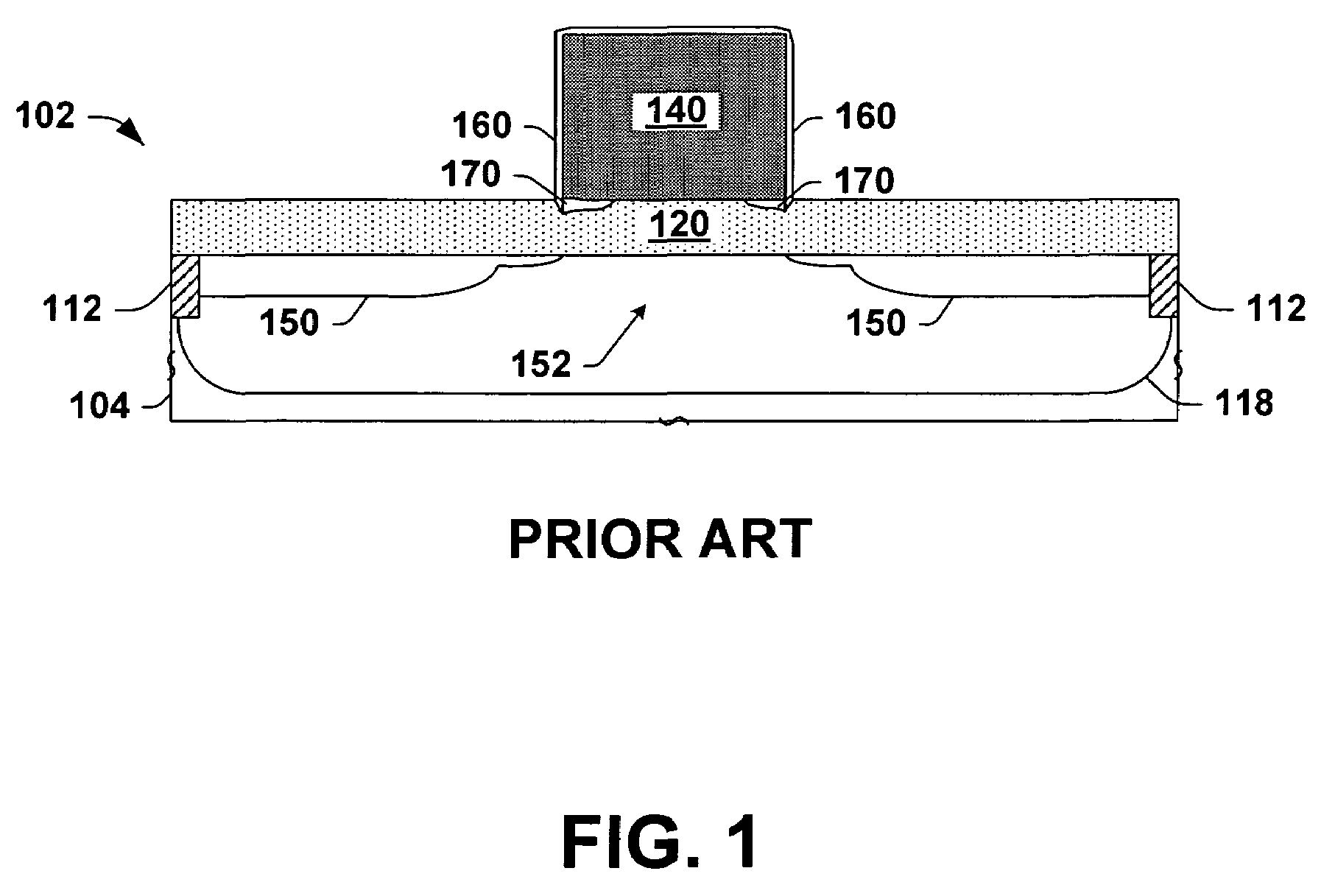
[0028]Semiconductor fabrication processes for conventional metal oxide semiconductor...


PUM


Abstract

Methods are disclosed that fabricating semiconductor devices with high-k dielectric layers. The invention removes portions of deposited high-k dielectric layers not below gates and covers exposed portions (e.g., sidewalls) of high-k dielectric layers during fabrication with an encapsulation layer, which mitigates defects in the high-k dielectric layers and contamination of process tools. The encapsulation layer can also be employed as an etch stop layer and, at least partially, in comprising sidewall spacers. As a result, a semiconductor device can be fabricated with a substantially uniform equivalent oxide thickness.

Description

FIELD OF INVENTION[0001]The present invention relates generally to semiconductor devices and more particularly to methods for fabricating high-k dielectrics and integrating high-k dielectrics into semiconductor device fabrication.BACKGROUND OF THE INVENTION[0002]Field effect transistors (FETs) are widely used in the electronics industry for switching, amplification, filtering, and other tasks related to both analog and digital electrical signals. Most common among these are metal-oxide-semiconductor field-effect transistors (MOSFET or MOS), in which a gate is energized to create an electric field in an underlying channel region of a semiconductor body, by which electrons are allowed to travel through the channel between a source region and a drain region of the semiconductor body. Complementary MOS (CMOS) devices have become widely used in the semiconductor industry, wherein both n-channel and p-channel (NMOS and PMOS) transistors are used to fabricate logic and other circuitry.[000...

Claims


Application Information

Patent Timeline
Patent Type & Authority Patents(United States)
IPC IPC(8): H01L21/336H01L21/28H01L21/8242H01L29/51
CPCH01L21/28176H01L21/28194H01L29/6656H01L29/6659H01L29/518H01L29/517
Inventor ROTONDARO, ANTONIO L. P.MERCER, DOUGLAS E.COLOMBO, LUIGIVISOKAY, MARK ROBERTBU, HAOWENBEVAN, MALCOLM JOHN
Owner TEXAS INSTR INC
Why Eureka
Try Eureka