Display unit

a display unit and display technology, applied in the field of display units, can solve the problems of unit reducing the transmittance of light from the organic el layer, the ineffective removal of external light, and the inability of the color filter to suppress the reflection of the r, g and b light components of the external light, so as to achieve the effect of significant improvement of contras

Inactive Publication Date: 2006-05-16
SONY CORP
View PDF14 Cites 10 Cited by
  • Summary
  • Abstract
  • Description
  • Claims
  • Application Information

AI Technical Summary

Benefits of technology

[0017](4) an R-light-transmitting filter and a B-light-transmitting filter are provided at the output side of light or at the incident side of e...

Problems solved by technology

However, these color filters cannot suppress the reflection of the R, G, and B light components of the external light.
(1) Although the display unit disclosed in Japanese Unexamined Patent Application Publication No. 9-127995 can effectively suppress the reflection of external light, the unit decreases the transmittance of light from the organic EL layer. Thus, the luminance is at most 50%.
(...

Method used


Image

  • Display unit
  • Display unit
  • Display unit

Examples


first embodiment

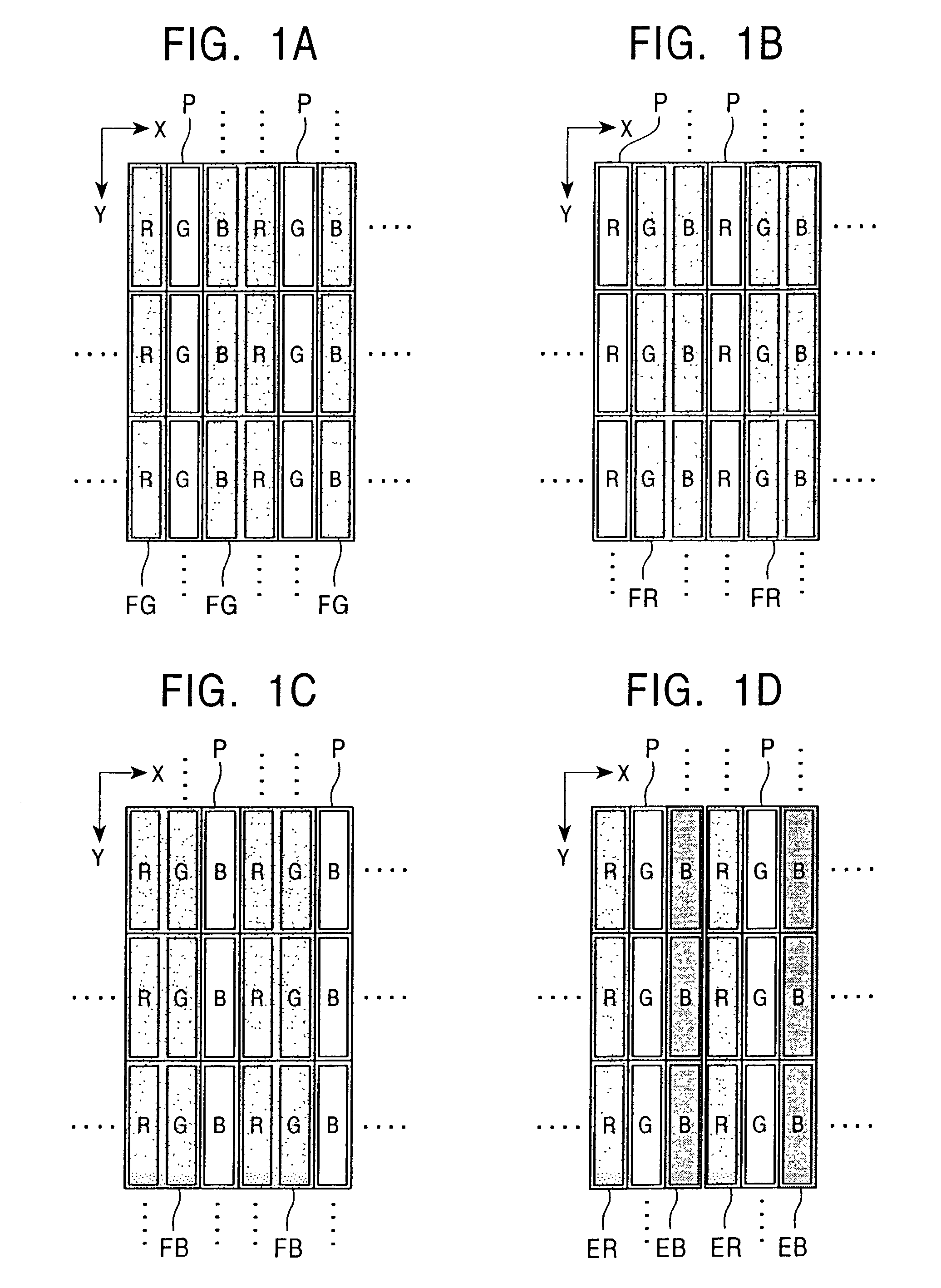
[0030]A first embodiment of the present invention will now be described in detail. Referring to FIG. 1A, R, G, and B light-emitting pixels are arranged in a predetermined sequence in a two-dimensional array. In this drawing, R, G, and B pixels are repeated in the X direction, whereas pixels of the same color are repeated in the Y direction. A combination of consecutive R, G, and B pixels in the X direction constitutes an image pixel P. In this embodiment, the R pixels and the B pixels each have a G-light-absorbing filter FG at the image display side (light output side or external-light incident side) thereof. The G pixels have no filters.

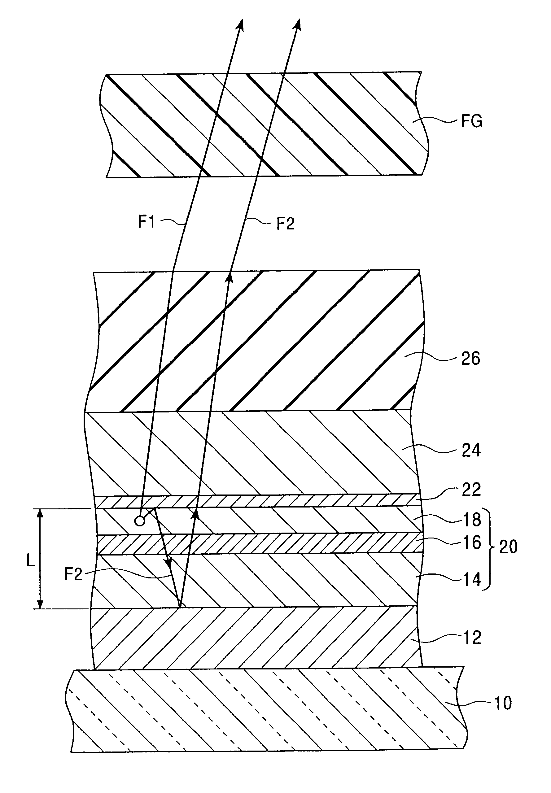
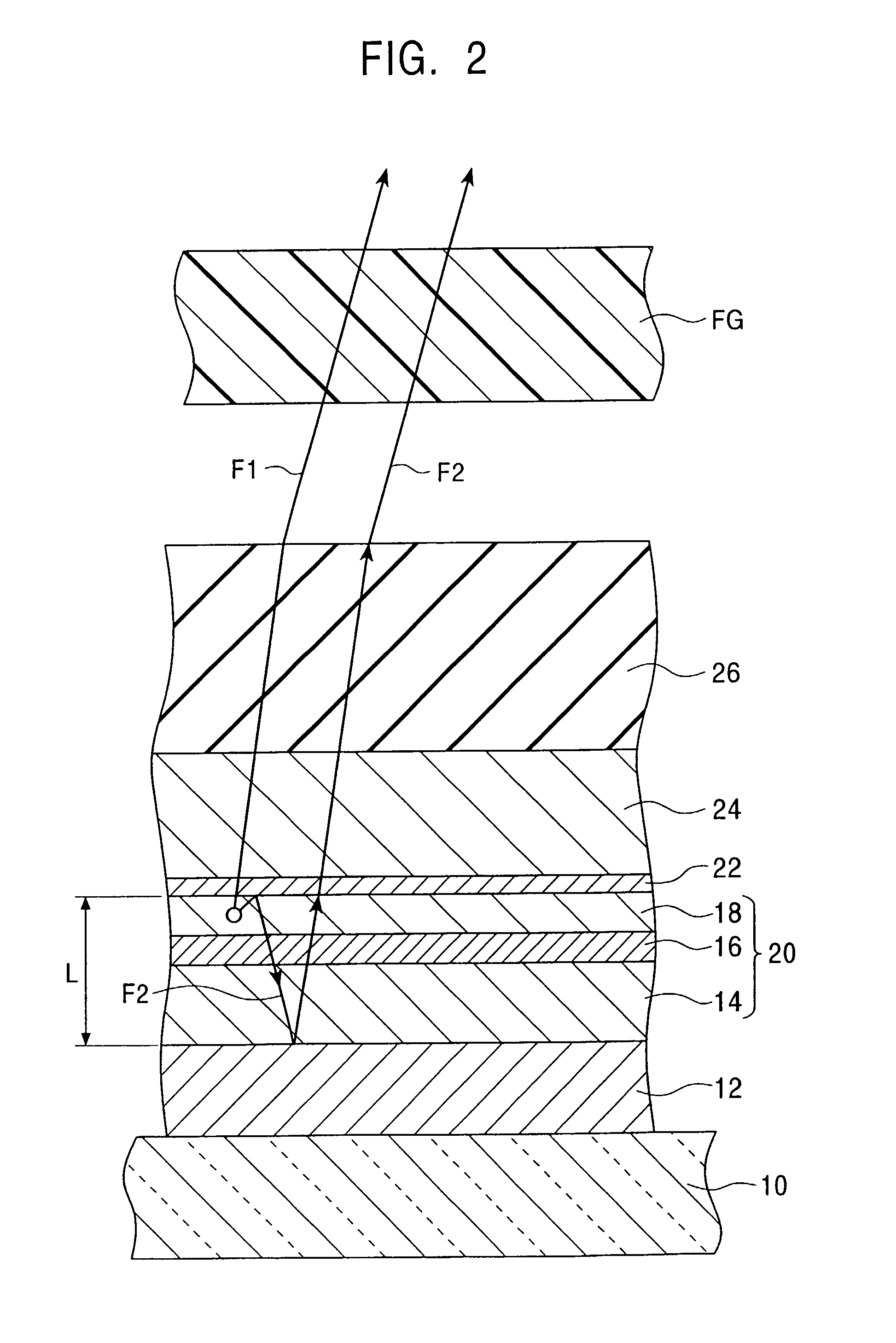
[0031]FIG. 2 shows a composite structure of an R or B light-emitting pixel. A reflective layer 12, which is composed of Pt, Au, Cr, or W and which also functions as an anode, is deposited on a glass substrate 10. A buffer layer 14 composed of m-MTDATA, 2-TNATA, or the like is deposited on the reflective layer 12, and a hole transport layer 16 compos...

second embodiment

[0056]Referring to FIG. 10, a second embodiment of the present invention will now be described. Components having the same functions as in the first embodiment are referred to with the same reference numerals. In this embodiment, light is output from the substrate side, unlike the first embodiment. A translucent reflective layer 50, a buffer layer 14, a hole transport layer 16, a luminescent layer 18, and a reflective layer 52 composed of aluminum or the like are deposited in that order on a substrate 10. Thus, the translucent reflective layer 50 is arranged at the substrate side. A G-light-absorbing filter FG is arranged on the substrate 10.

[0057]A fraction F11 of light emitted from the luminescent layer 18 of the organic EL layer 20 passes through the translucent reflective layer 50, transparent conductive layer 24, and the glass substrate 10 and is incident on the G-light-absorbing filter FG. Another fraction F11 of the light emitted from the luminescent layer 18 is reflected by ...

third embodiment

[0058]Referring to FIGS. 11A to 11D, a third embodiment of the present invention will now be described. In FIG. 11A, a G-light-absorbing filter FG is provided on a passivation film 26. In FIG. 11B, a G-light-absorbing filter FG is provided between a transparent conductive layer 24 and a passivation film 26. The only difference between these modifications and the first embodiment is the position of the G-light-absorbing filter FG. In the first embodiment, the luminescent layer 18 also functions as the electron transport layer. In FIG. 11C, both a luminescent layer 18A and an electron transport layer 18B are provided.

[0059]In the above embodiments, a reflective layer and a translucent reflective layer constitute an optical resonator structure. In FIG. 11D, no translucent reflective layer is provided. The light emitted from the organic EL layer 20 is directly incident on a G-light-absorbing filter FG, as shown by arrow F1, or is reflected by the reflective layer 12 and then is incident...


PUM


Abstract

A display unit has R, G, and B light-emitting pixels arranged in a predetermined sequence. The R pixels and the B pixels each have a G-light-absorbing filter at the image display side (light output side or external-light incident side) thereof. The G pixels have no filters. The R and B light-emitting pixels each have a composite structure including a reflective layer, an organic EL layer, and a translucent reflective layer. The translucent reflective layer and the reflective layer constitute an optical resonator that causes multiple interference of light. The transmittance of the G-light-absorbing filter is minimized at the G wavelength, at which the sensitivity of the naked eye is high, and maximized at the R and B wavelengths. Furthermore, the external light reflectance of each pixel is minimized at the G wavelength. This display unit significantly suppresses a decrease in contrast caused by external light without a decrease in luminance of an image.

Description

BACKGROUND OF THE INVENTION[0001]The present invention relates to display units and, more particularly, to an improvement in a display unit including an organic EL device.[0002]A typical organic electroluminescent (EL) device has a composite structure including an organic EL layer sandwiched by electrodes, one electrode being composed of a metal such as aluminum, the other being a transparent electrode composed of, for example, indium tin oxide (ITO). A proportion of light emitted from the organic EL layer is directly output through the transparent electrode, while light output toward the metal electrode is reflected by the metal electrode and output through the transparent electrode. External light incident on the organic EL layer through the transparent electrode is also reflected by the metal electrode and then output through the transparent electrode. That is, the external light is added to the internal light emitted from the organic EL layer for forming an image. Thus, under ex...

Claims


Application Information

Patent Timeline
IPC IPC(8): H05B33/00G09F9/00H05B33/02G09F9/30H01L27/32H01L51/50H01L51/52H05B33/12H05B33/22H05B33/26
CPCH01L27/3211H01L51/5281H01L51/5265H01L27/322H10K59/35H10K59/38H10K59/8791H10K59/876H05B33/22H10K50/86H10K50/852
Inventor YAMADA, JIROIWASE, YUICHI
Owner SONY CORP
Why Eureka
Try Eureka