Vacuum device having a getter

a vacuum device and getter technology, applied in vacuum obtaining/maintenance, positive displacement liquid engines, machines/engines, etc., can solve the problems of increasing the complexity and difficulty of assembly, increasing the size of the package, and the inability to produce either a thicker or a larger packag

Active Publication Date: 2006-05-16
SAMSUNG ELECTRONICS CO LTD
View PDF26 Cites 17 Cited by
  • Summary
  • Abstract
  • Description
  • Claims
  • Application Information

AI Technical Summary

Problems solved by technology

One of the major problems with vacuum packaging of electronic devices is the continuous outgassing of hydrogen, water vapor, carbon monoxide, and other components found in ambient air, and from the internal components of the electronic device.
Although this approach provides an alternative to inserting a ribbon or cartridge inside the vacuum package, it still results in the undesired effect of producing either a thicker or a larger package.
Such an approach leads to increased complexity and difficulty in assembly as well as increased package size.
Especially for small electronic devices with narrow gaps, the incorporation of a separate cartridge also results in a bulkier package, which is undesirable in many applications.
Further, the utilization of a separate compartment increases the cost of manufacturing because it is a separate part that requires accurate positioning, mounting, and securing to another component part to prevent it from coming loose and potentially damaging the device.
Although this approach provides an efficient means of obtaining a uniform vacuum within the vacuum package, it also will typically result in the undesired effect of producing a thicker package, because of the need to maintain a reasonable gap between the bottom surface of the substrate and the top surface of the getter material to allow for reasonable pumping action.
In addition, yields typically decrease due to the additional processing steps necessary to produce the uniform distribution of pores.
The ability, to optimize the gettering performance of non-evaporable getters may open up a wide variety of applications that are currently either impractical, or are not cost effective.

Method used


Image

  • Vacuum device having a getter
  • Vacuum device having a getter
  • Vacuum device having a getter

Examples


Embodiment Construction

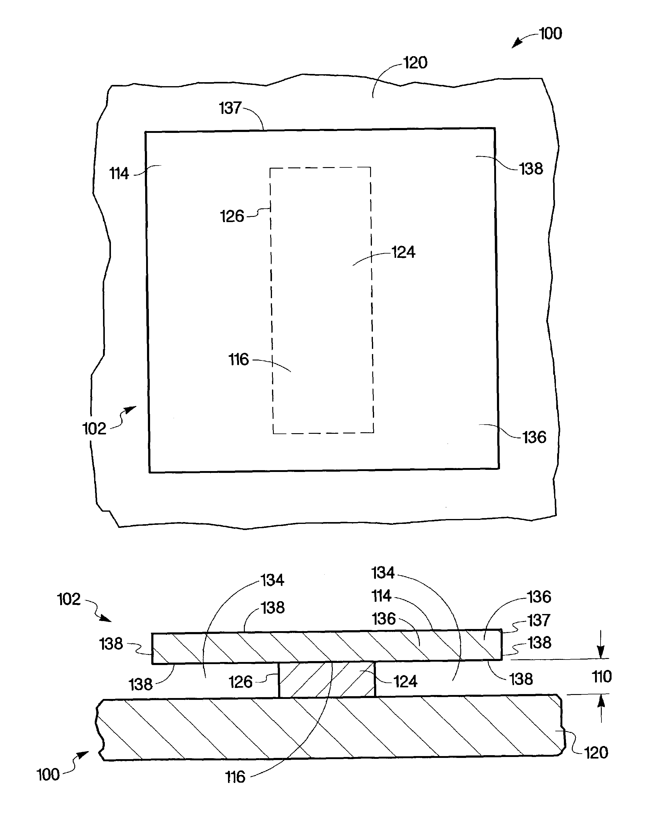
[0018]Referring to FIG. 1a, an embodiment of vacuum device 100 of the present invention, in a top view, is shown. Getter structure 102 is utilized as a vacuum pump to maintain a vacuum or pressure below atmospheric pressure for vacuum device 100. Vacuum device 100 may be incorporated into any device utilizing a vacuum, such as, electronic devices, MEMS devices, mechanical devices, and optical devices to name a few. As electronic manufacturers look for higher orders of integration to reduce product costs, typically, package sizes get smaller leaving less room for getter material. Electronic circuits and devices disposed on a wafer or substrate limit the area available for getter structures. This limited area increases the desire to fabricate getters with high surface area structures having a small footprint on the substrate or wafer. In addition, in those embodiments utilizing wafer-level packaging, a technique that is becoming more popular for its low costs, placing a higher surface...


PUM


Abstract

A vacuum device, including a substrate and a support structure having a support perimeter, where the support structure is disposed over the substrate. In addition, the vacuum device also includes a non-evaporable getter layer having an exposed surface area. The non-evaporable getter layer is disposed over the support structure, and extends beyond the support perimeter, in at least one direction, of the support structure forming a vacuum gap between the substrate and the non-evaporable getter layer increasing the exposed surface area.

Description

BACKGROUNDDESCRIPTION OF THE ART[0001]The ability to maintain a low pressure or vacuum for a prolonged period in a microelectronic package is increasingly being sought in such diverse areas as displays technologies, micro-electro-mechanical systems (MEMS) and high density storage devices. For example, computers, displays, and personal digital assistants may all incorporate such devices. Many vacuum packaged devices utilize electrons to traverse some gap to excite a phosphor in the case of displays, or to modify a media to create bits in the case of storage devices, for example.[0002]One of the major problems with vacuum packaging of electronic devices is the continuous outgassing of hydrogen, water vapor, carbon monoxide, and other components found in ambient air, and from the internal components of the electronic device. Typically, to minimize the effects of outgassing one uses gas-absorbing materials commonly referred to as getter materials. Generally a separate cartridge, ribbon,...

Claims


Application Information

Patent Timeline
Patent Type & Authority Patents(United States)
IPC IPC(8): H01J17/24H01J19/70H01J61/26F04B37/02H01J7/18H01K1/52
CPCF04B37/02H01J19/70H01J7/186
Inventor RAMAMOORTHI, SRIRAMCHEN, ZHIZHANGLIEBESKIND, JOHNENCK, RONALD L.SHIH, JENNIFER
Owner SAMSUNG ELECTRONICS CO LTD
Why Eureka
Try Eureka