
Internal voltage generator

a technology of internal voltage generator and generator, which is applied in the direction of pulse generator, pulse technique, instruments, etc., can solve the problems of increasing internal voltage, increasing power consumption continuously consuming power in internal voltage generator, so as to reduce power consumption

Inactive Publication Date: 2006-05-16
SK HYNIX INC
View PDF15 Cites 35 Cited by
  • Summary
  • Abstract
  • Description
  • Claims
  • Application Information

AI Technical Summary

Benefits of technology

The present invention aims to provide an internal voltage generator that can reduce power consumption and restrict abnormal variations of an internal voltage resulting from a leakage current generated in a driving transistor in a turn-off state. The internal voltage generator includes a comparator, a driving transistor, a back bias circuit, and a controller. The comparator receives a reference voltage and the internal voltage and compares them. The driving transistor receives the output signal from the comparator and outputs the internal voltage. The back bias circuit supplies a predetermined potential of back bias voltage to the well region of the driving transistor. The controller receives the output signal from the comparator and controls the operation of the back bias circuit. The back bias circuit includes a MOS transistor. The invention can reduce power consumption and restrict abnormal variations of the internal voltage.

Problems solved by technology

As a result, power is continuously consumed in the internal voltage generator.
1. Power consumption increases in the internal voltage generator due to a high speed tendency of the semiconductor device.
2. In spite of high integration of the semiconductor device, driving capability must be improved by using a large-sized driving transistor to generate a stable internal voltage.
3. As the driving voltage of the semiconductor device is lowered, a threshold voltage of the driving transistor is also lowered. When the threshold voltage is lowered, although the driving transistor must maintain a turn-off state, a leakage current is generated, to unnecessarily increase the internal voltage. The leakage current is Io*exp(Vgs−Vth) / nkT in the turn-off state. That is, when the size of the driving transistor increases and the threshold voltage decreases, the leakage current increases.

Method used


Image

  • Internal voltage generator
  • Internal voltage generator
  • Internal voltage generator

Examples


first embodiment

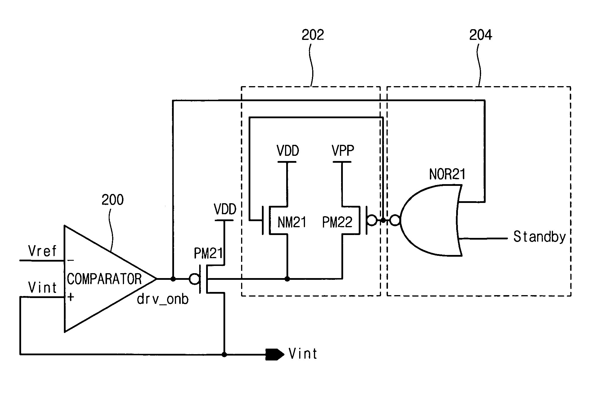
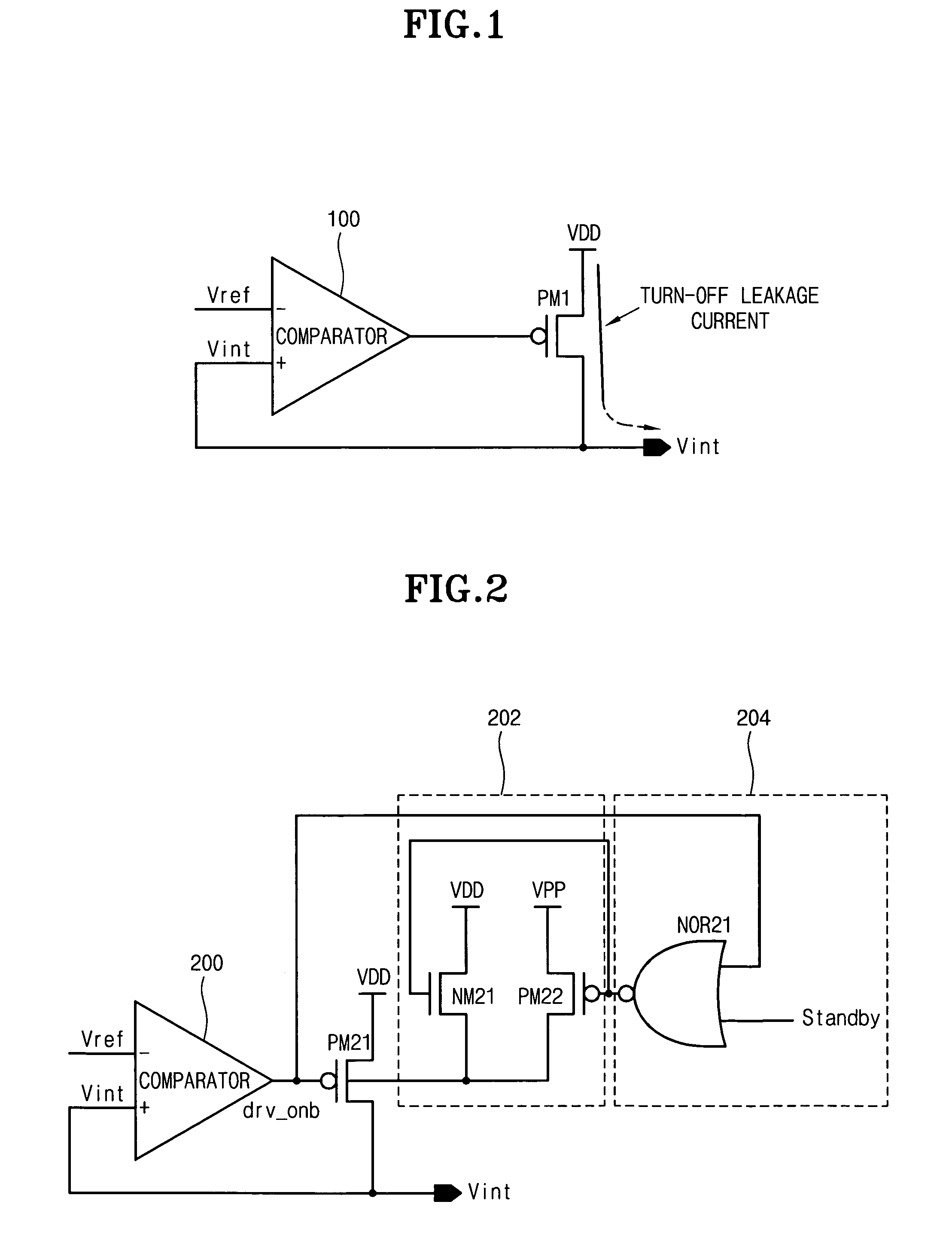
[0025]FIG. 2 is a circuit diagram illustrating an internal voltage generator in accordance with the present invention.

[0026]As illustrated in FIG. 2, the internal voltage generator for generating an internal voltage for a semiconductor device includes a comparator 200, a driving transistor PM21, a back bias circuit 202 and a controller 204.

[0027]The comparator 200 receives a reference voltage Vref through its first input terminal, namely a negative terminal, receives the internal voltage Vint through its second input terminal, namely a positive terminal, and compares the reference voltage Vref with the internal voltage Vint. The comparator 200 can be embodied as various circuits by those skilled in the art.

[0028]The driving transistor PM21 receives the output signal from the comparator 200 through its gate terminal. A first terminal of the driving transistor PM21, namely a source terminal is coupled to a driving voltage VDD, and a second terminal of the driving transistor PM21, name...

second embodiment

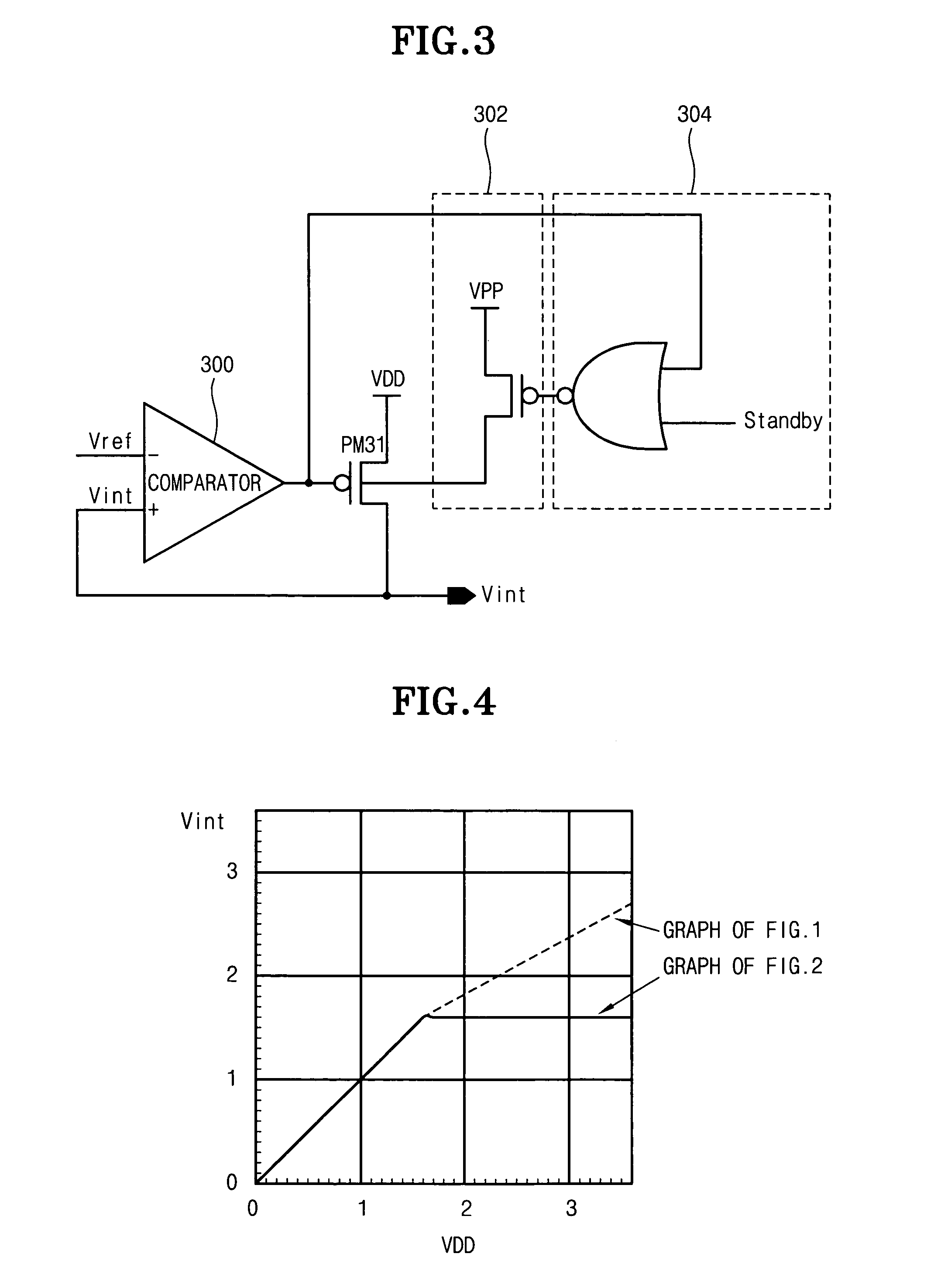
[0038]FIG. 3 is a circuit diagram illustrating an internal voltage generator in accordance with the present invention.

[0039]As depicted in FIG. 3, the internal voltage generator for generating an internal voltage for a semiconductor device includes a comparator 300, a driving transistor PM31, a back bias circuit 302 and a controller 304.

[0040]The internal voltage generator of FIG. 3 is identical to the internal voltage generator of FIG. 2 except that the back bias circuit 302 merely includes PMOS transistors. Thus, the circuit operation of FIG. 3 is basically identical to that of FIG. 2.

[0041]FIG. 4 is a graph showing variations of the internal voltage by the leakage current.

[0042]In FIG. 4, a transverse axis shows the driving voltage VDD, and an ordinate axis shows the internal voltage Vint. A dotted line shows the internal voltage in the conventional circuit of FIG. 1, and a solid line shows the internal voltage in the circuit of the present invention.

[0043]As shown in FIG. 4, in ...


PUM


Abstract

The present invention discloses an internal voltage generator which can restrict abnormal variations of an internal voltage resulting from a leakage current generated in a driving transistor. The internal voltage generator includes a comparator for receiving a reference voltage through its first input terminal, receiving the internal voltage through its second input terminal, and comparing the reference voltage with the internal voltage, a driving transistor for receiving the output signal from the comparator through its gate terminal, a first terminal of which being coupled to a driving voltage, a second terminal of which being an output terminal for outputting the internal voltage, a back bias circuit for supplying a predetermined potential of back bias voltage to a well region of the driving transistor, and a controller for receiving the output signal from the comparator, and controlling the operation of the back bias circuit. The second terminal of the driving transistor is feedback-coupled to the second input terminal of the comparator. When the driving transistor is turned off according to the output signal from the comparator, the controller for receiving the output signal from the comparator supplies the predetermined potential of back bias voltage to the well region of the driving transistor by driving the back bias circuit.

Description

BACKGROUND OF THE INVENTION[0001]1. Field of the Invention[0002]The present invention relates to an internal voltage generator, and more particularly to, an internal voltage generator which can restrict abnormal variations of an internal voltage resulting from a leakage current generated in a driving transistor.[0003]2. Description of the Related Art[0004]FIG. 1 is a circuit diagram illustrating a conventional internal voltage generator.[0005]Referring to FIG. 1, the conventional internal voltage generator includes a comparator 100 and a PMOS driving transistor PM1. The comparator 100 compares a reference voltage Vref inputted to its negative terminal with an internal voltage Vint inputted to its positive terminal, and outputs the comparison result. The PMOS driving transistor PM1 is turned on / off according to the output signal from the comparator 100. The PMOS driving transistor PM1 has its source terminal connected to a driving voltage VDD. When the PMOS driving transistor PM1 is ...

Claims


Application Information

Patent Timeline
Patent Type & Authority Patents(United States)
IPC IPC(8): G05F1/10G11C5/14H02J1/00
CPCG11C5/147G02B5/02G11C5/14
Inventor JANG, KYEONG SIK
Owner SK HYNIX INC
Learn More