Method and device for converting a quantized digital value

Inactive Publication Date: 2006-05-16
EADS SECURE NETWORKS
4 Cites 2 Cited by

AI-Extracted Technical Summary

Problems solved by technology

However, it may arise that this resolution is insufficient for representing some or all of the digital signals of the system.
In this case, the situation may be encountered in which a quantization error affecting the digital constant (this error being systematic inasmuch as it does not vary) exceeds the maxi...

Method used

[0104]In a digitally modulated synthesizer, the frequency divider 14 includes an input for controlling the division ratio. This ratio is fixed by the value stored in a specific accumulator. In order to prevent spurious lines, due to periodicity of the division ratio changes from N to N+1 and back again, from occurring in the spectrum of the output signal Sout, however, a DMS known in the prior art furthermore includes a modulator 15 of the digital/digital Σ-Δ modulator type.
[0108]According to the invention, the value Sch2 is delivered by a converter device 18 as described above with reference to FIGS. 2 to 6, on the basis of a digital value Schq1 stored in an appropriate register. The quantized values Sch1 and Sch2 correspond to a real value, namely the central frequency of the channel, denoted below by Fch. The real...

Benefits of technology

[0044]It can be seen that the effect of the invention is to implement relation (9) by using relation (10). It therefore makes it possible to convert the digital value Sq1 into a digital value Sq2, which are information quantized according to different respective quantization coefficients Cq1 and Cq2 and which both correspond to the same real information S, without any restrictive assumption being made about the relation between one of these quantization coefficients and the other.
[0045]The invention thus makes it possible to reduce the quantization error affecting a variable or constant real value. Specifically, it is sufficient to choose the first quantization coefficient Cq1 so as to minimize the quantization error affecting the digital value Sq1, and to convert this value by delivering it as a digital input value to a device according to the invention, in order to obtain a digital output value Sq2 quantized according to a second quantization coefficient Cq2, which will be chosen as being that of the quantization of the subsystem needing to use the digital input value. The quantization error affecting the digital value Sq2 can thus be reduced without any constra...

Abstract

The invention concerns a method and a device for converting an input digital value quantized in accordance with a first quantization factor and encoded on at most n1 bits, into an output digital value quantized in accordance with a second quantization factor and encoded on at most n2 bits. The method comprises the steps of: multiplying the input digital value by an integer B, encoded on at most β bits, so as to generate an intermediate digital value; and dividing, in fixed point, the first intermediate digital value by the number 2α, where α is an integer not greater than n1+β, generating the output digital value. The number B/2α is substantially equal to the ratio of the second quantization factor over the first quantization factor. Additionally, the divider means comprise a Sigma-Delta modulator.

Application Domain

Technology Topic

First quantizationDelta modulation +4

Image

  • Method and device for converting a quantized digital value
  • Method and device for converting a quantized digital value
  • Method and device for converting a quantized digital value

Examples

  • Experimental program(3)

Example

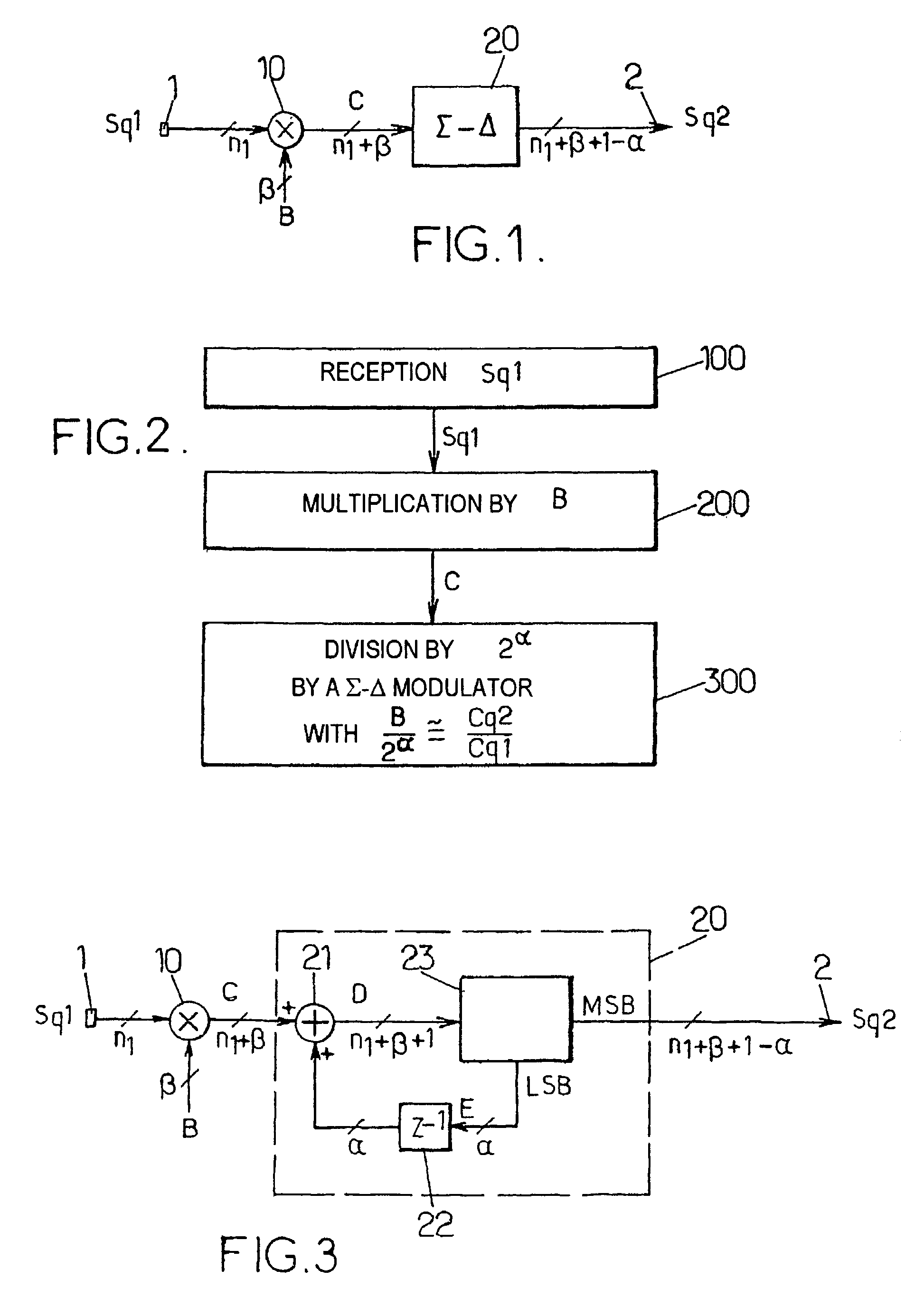
[0085]The diagram in FIG. 3 illustrates a first embodiment of a device according to the invention, which is suitable for carrying out a first variant of the method.
[0086]In this first embodiment, the sigma-delta modulator 20 comprises means 21 such as a digital adder, which receive as input the first intermediate digital value C as a first operand, on the one hand, and a digital error value E as a second operand, on the other hand. The latter is encoded over at most α bits. The means 21 deliver as output a second intermediate digital value D encoded over at most n1+β+1 bits.
[0087]The device further comprises selection means 23, such as a digital discriminator, for selecting the n2 most significant bits of the second intermediate digital value D as the digital output value Sq2, and for selecting the α least significant bits of said second intermediate digital value D as the digital error value E. It follows that n2 is equal to n1+β+1−α. The means 23 receive the value D as input and deliver the value Sq2 as well as the value E as output.
[0088]A digital discriminator is a circuit which separates the k high-significance bits and the j low-significance bits of a given digital input value in order to generate two digital output values, encoded respectively over k bits and over j bits and each having as its value the value corresponding respectively to said k high-significance bits and to the j low-significance bits. Here, the discriminator 23 separates the n1+β+1−α most significant bits of the second intermediate digital value D, on the one hand, and the α least significant bits of the value D, on the other hand.

Example

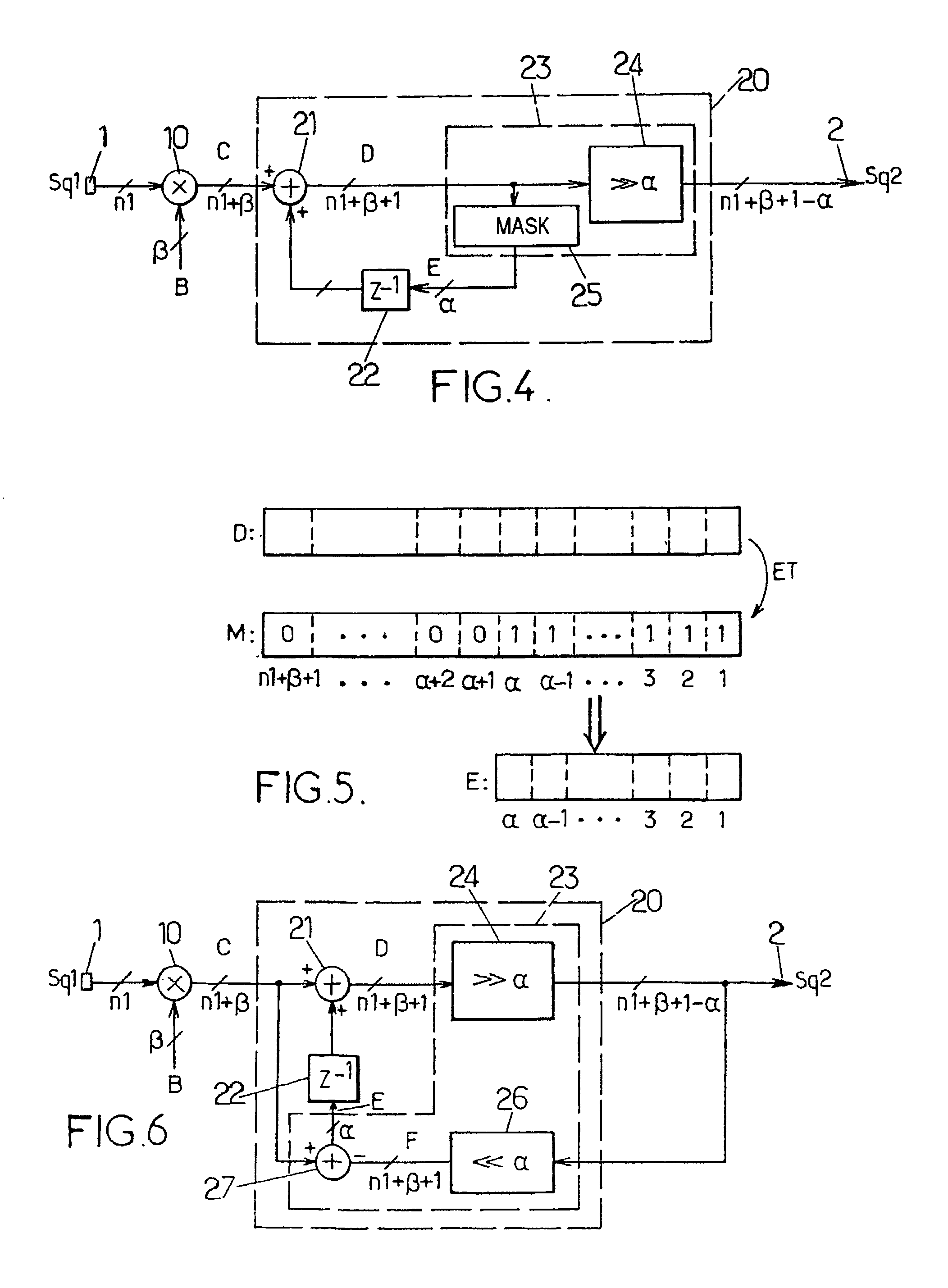
[0089]The diagram in FIG. 4 illustrates a second embodiment of a device according to the invention, which is suitable for carrying out a second variant of the method.
[0090]In this second embodiment, the selection means 23 of the device comprise an operator 24 for shifting to the right by α bits. Such an operator is formed, for example, with the aid of a properly controlled shift register. This operator 24 receives as input the n1+β+1 bits of the second intermediate digital value D. It delivers as output the n1+β+1−α most significant bits of the second intermediate digital value D as a digital output value Sq2.
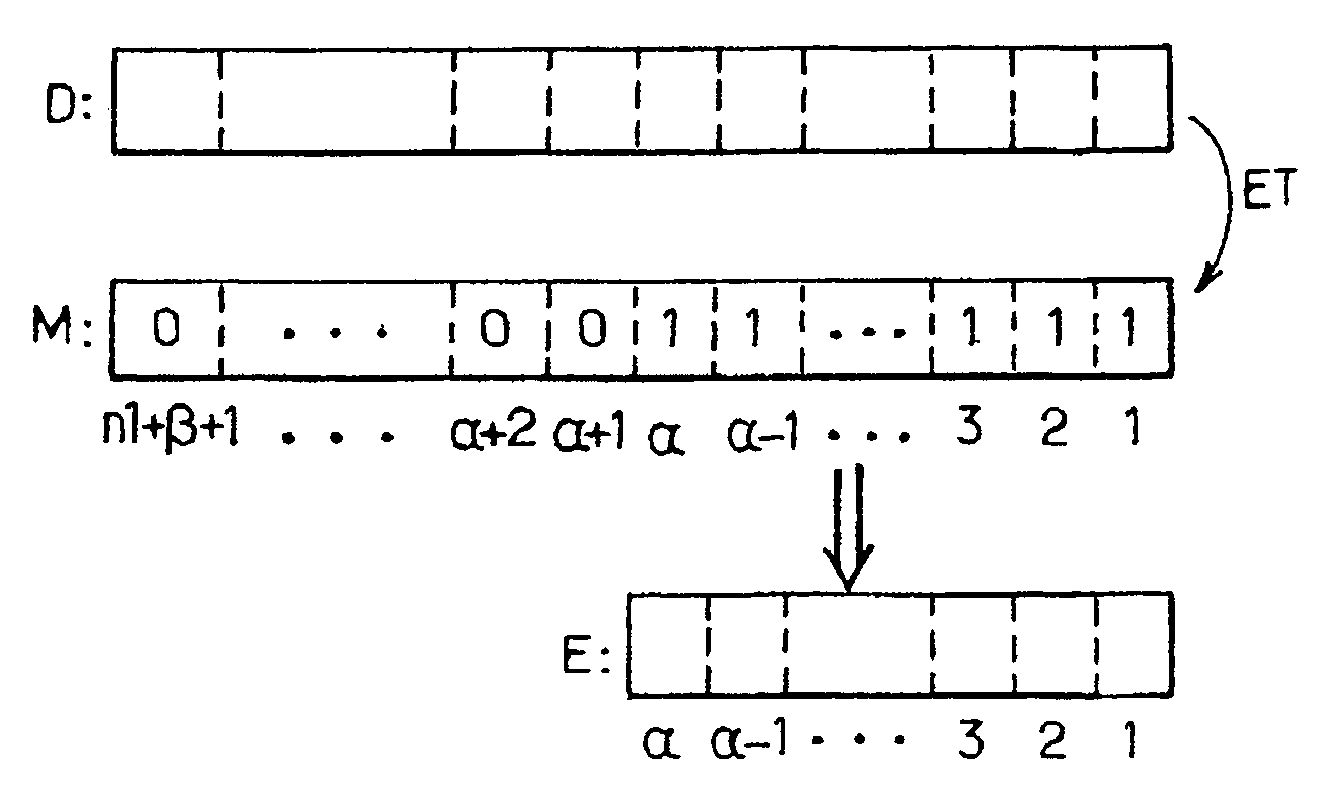
[0091]The selection means 23 furthermore comprise means 25 for applying a mask to the second intermediate digital value D.
[0092]Such a mask is represented in FIG. 5 with the reference M. It is a digital value stored in an appropriate register and having at most n1+β+1 bits, the n1+β+1−α most significant bits of which are equal to the logical value 0 and the α least significant bits of which are equal to the logical value 1. When it is combined with the second intermediate digital value D in an operation of the logical AND type, it makes it possible to select the α least significant bits of said second intermediate digital value D.
[0093]Stated otherwise, the means 25 receive as input the n1+β+1 bits of the second intermediate digital value D. They deliver as output the n1+β+1−α most significant bits of the second intermediate digital value D as the digital error value E.

Example

[0094]The diagram in FIG. 6 illustrates a third embodiment of a device according to the invention, which is suitable for carrying out a third variant of the method.
[0095]In this third embodiment, the selection means 23 of the device still comprise an operator 24 for shifting to the right by α bits, which has the same function as the operator 24 of the device in FIG. 4.
[0096]The selection means 23 further comprise an operator 26 for shifting to the left by α bits, which receives as input the n1+β+1−α bits of the digital output value Sq2 and delivers as output a third intermediate digital value F, encoded over at most n1+β+1 bits. The operator 26 is, for example, a properly controlled shift register. They furthermore comprise an operator 27 for taking the difference between the intermediate digital values F and C. The operator 27 is, for example, a digital subtracter. It receives the third intermediate digital value F as a first operand, and the first intermediate digital value C as a second operand. It delivers as output the digital error value E.
[0097]In each of the three embodiments described above with reference to FIGS. 3, 4 and 6, the device preferably comprises an operator 22 that applies a unitary delay to the digital error value E for synchronization reasons. Stated otherwise, the error signal E is delivered to the input of the adder means 21 through a unitary delay operator 22.
[0098]FIG. 6 shows the diagram of a digitally modulated frequency synthesizer, more commonly referred to by the term DMS, which incorporates a device according to the invention.
[0099]Such a circuit can be used for generating a frequency- or phase-modulated radiofrequency signal (in the UHF band lying between 400 and 600 MHz). Applications may be found for it in the radio transmitters or transceivers of a radiocommunication system, particularly in the base stations and/or the mobile terminals of such a system.
[0100]A DMS has a structure which is derived from the structure of a fractional N frequency synthesizer, and makes it possible to generate a frequency- or phase-modulated periodic signal.
[0101]The DMS includes a phase-locked loop or “PLL”, comprising a phrase/frequency comparator 11 or “PFC”, a loop filter 12 such as an integrator, and a voltage controlled oscillator 13 or “VCO” in series in a forward channel, and as well as a frequency divider 14 in a return channel. The VCO delivers as output a signal Sout which is the output signal of the DMS, the instantaneous frequency of which is fout. The PFC receives at a first input a reference signal Sref having a reference frequency fref, and at a second input a signal Sdiv delivered by the frequency divider 14 on the basis of the signal Sout.
[0102]For conventional fractional N synthesis, the frequency divider 14 is a variable-ratio divider making it possible to produce the signal Sdiv by dividing the frequency fout of the signal Sout by a division ratio, which alternately has the value of an integer N for a part of the time T1 and the integer N+1 for the rest of the time T2. In this way, the frequency fout of the output signal Sout is given as a function of the frequency fref of the reference signal Sref by:
[0103] f out = ( N + T1 T1 + T2 ) × f ref ( 14 )
[0104]In a digitally modulated synthesizer, the frequency divider 14 includes an input for controlling the division ratio. This ratio is fixed by the value stored in a specific accumulator. In order to prevent spurious lines, due to periodicity of the division ratio changes from N to N+1 and back again, from occurring in the spectrum of the output signal Sout, however, a DMS known in the prior art furthermore includes a modulator 15 of the digital/digital Σ-Δ modulator type.
[0105]The modulator 15 includes an input which receives a digital frequency- or phase-modulation value Smod encoded over k bits, and an output which delivers a digital value S′mod, corresponding to the processed value Smod and encoded over j bits. The output of the modulator 15 is connected to a first input of a digital adder 16, the second input of which receives a digital value No that defines the bottom of the frequency band addressed by the synthesizer. The output of the adder 16 delivers a digital value Sc. It is connected to the control input of the divider 14 in order to deliver the value Sc to it.
[0106]The DMS also comprises a second digital adder 17, a first input of which receives a digital value Sinfo and a second input of which receives a digital value Sch2. The output of the adder 17 delivers the aforementioned digital frequency- or phase-modulation value Smod. The digital value Sinfo contains the modulation information (modulating signal), that is to say the useful information to be transmitted. The digital value Sch2 corresponds to the central frequency of the radio channel (after the aforementioned value No has been added).
[0107]The digital values Sinfo, Sch2, Smod and S′mod and No are values that are quantized according to a quantization coefficient Cq2 of the digital system constituted by the DMS.
[0108]According to the invention, the value Sch2 is delivered by a converter device 18 as described above with reference to FIGS. 2 to 6, on the basis of a digital value Schq1 stored in an appropriate register. The quantized values Sch1 and Sch2 correspond to a real value, namely the central frequency of the channel, denoted below by Fch. The real value Fch is constant, because the central frequency of the channel is constant. If the device 18 was not there, the real value Fch would be directly quantized according to the quantization coefficient Cq2 of the digital system constituted by the DMS. However, the DMS presented here incorporates a device 18 according to the invention in order to reduce the quantization error affecting the quantized digital value corresponding to the real value Fch (which is a systematic error since this value is constant). Stated otherwise, the DMS comprises a device 18 for converting the digital value Sch1 into a digital value Sch2, which is quantized according to the quantization coefficient Cq2 of the digital system constituted by the DMS.
[0109]To apply that which has been described above, a choice is therefore made to implement a converter device 18 of the type described above, for which Cq1 is equal to unity (Cq1=1, because the real value Fch is integer) and for which Cq2 is the quantization coefficient of the quantization of the DMS.
[0110]A numerical example for illustrating the advantages offered by the invention in this application will be given below. In this example: [0111] Fref=9.6 MHz (megahertz); [0112] k=22; [0113] j=4; [0114] Fch=400017.5 kHz (kilohertz); [0115] No=round(395 MHz/Fref); [0116] ed=4 Hz (hertz).
[0117]The frequency resolution of such a DMS is given by
[0118] F ref 2 k - j ,
where k is the number of bits at the input of the sigma-delta modulator 15, and where j is the number of bits at the output of this modulator. The frequency resolution of the DMS, that is to say
[0119] 1 Cq2 ,
is therefore:
[0120] 1 Cq2 = F ref 2 k - j = 9.6 · 10 6 2 18 ≈ 36.62 ⁢ ⁢ Hz
[0121]The value Fmin, corresponding to the bottom of the frequency band addressed by the DMS, is determined by the digital value No according to the relation Fmin=No×Fref. Here, therefore, Fmin=41×9.6·106=393.6 MHz.
[0122]Let us first consider what the situation would be without the device 18 according to the invention, that is to say if Sch1=Sch2. We would have:
Fch2=round[(Fch−Fmin).Cq2]=175241
[0123]The systematic quantization error affecting the central frequency of the radio channel would therefore be:
[0124] e = F ch - ( Fch2 Cq2 + F min )
[0125]i.e.:
[0126] e = 400017.5 · 10 3 - ( 175241 Cq2 + 393.6 · 10 6 ) = - 17.08 ⁢ ⁢ Hz
[0127]This value exceeds (in absolute value) the acceptable error ed.
[0128]Let us now consider what happens with the conversion device 18 according to the invention. Since the signal intended to be represented is integer, we have Cq1=1.
[0129]The following approximation is chosen:
[0130] Cq2 ≈ B 2 α = 229065 2 23 .
In other words, a choice is made to implement a device according to the invention with B=229065 and α=23.
[0131]The quantization error can be determined by using the relation (13) given in the introduction, which is valid in the case when the real digital value at the input of the device (here, the constant value Fch−Fmin) is an integer. It will be recalled that this relation is then written:
[0132] e = S · ɛ = S · Cq1 Cq2 ⁢ ⁢ B 2 α ⁢ 1 ≅ 2.17 ⁢ ⁢ Hz
[0133]where S denotes the real digital value at the input of the device (here Fch).
[0134]Whence it follows that e≅2.17 Hz. The goal of a quantization error less than 4 Hz affecting the value of the central frequency of the radio channel has therefore indeed been achieved, without having to modify the quantization of the system. Here, the invention makes it possible to reduce the systematic quantization error affecting the value of the central frequency of the radio channel from 17 Hz to 2 Hz.
[0135]A better result could be obtained by increasing the precision of the approximation for
[0136] Cq2 Cq1 ,
but at the cost of increasing the number β and the number α.

PUM

no PUM

Description & Claims & Application Information

We can also present the details of the Description, Claims and Application information to help users get a comprehensive understanding of the technical details of the patent, such as background art, summary of invention, brief description of drawings, description of embodiments, and other original content. On the other hand, users can also determine the specific scope of protection of the technology through the list of claims; as well as understand the changes in the life cycle of the technology with the presentation of the patent timeline. Login to view more.

Similar technology patents

Feeder terminal device and signal acquisition calculation and line selection method thereof

PendingCN112557804AImprove acquisition accuracy and speedReduce quantization errorFault location by conductor typesCircuit interrupters testingDigital conversionFeeder line
Owner:SHANDONG ELECTRICAL ENG & EQUIP GRP XINNENG TECH CO LTD

Method and device for quantizing local features of picture into visual vocabularies

ActiveCN103020231AReduce quantization errorImprove robustnessSpecial data processing applicationsRelationship - FatherConfidence factor
Owner:BEIJING BAIDU NETCOM SCI & TECH CO LTD

Digital adaptive hysteresis system

InactiveUS20050286380A1Reduce quantization errorOutput errorTelevision system detailsDigital technique networkSelf adaptiveRounding
Owner:CIRRUS LOGIC INC

ITQ algorithm-based Indonetic similar news recommendation method

ActiveCN109992716AReduce computation and memory overheadReduce quantization errorWeb data indexingSpecial data processing applicationsTheoretical computer scienceData science
Owner:UNIV OF ELECTRONIC SCI & TECH OF CHINA

Classification and recommendation of technical efficacy words

  • Minimize error
  • Reduce quantization error

Apparatus and method for managing prescription benefits

InactiveUS7155397B2Minimize errorCost-optimizedFinanceDigital data processing detailsCase recordsCase note
Owner:EXPRESS SCRIPTS STRATEGIC DEV INC

Dictionary learning static image lossy compression method based on minimum quantization error criterion

ActiveCN107170020AReduce coding costsReduce quantization errorCode conversionImage codingDictionary learningSparse coefficient
Owner:NORTHWESTERN POLYTECHNICAL UNIV

Low-power time-to-digital converter

ActiveCN110174834AHigh precisionReduce quantization errorTime-to-digital convertersVIT signalsCapacitance
Owner:FUDAN UNIV

Neural network optimization method and related equipment

PendingCN111950700AReduce quantization errorEfficient in training and useGeometric image transformationCharacter and pattern recognitionEngineeringAlgorithm
Owner:HUAWEI TECH CO LTD
Why Eureka
Try Eureka