Display and its driving method

Inactive Publication Date: 2006-05-23
PANASONIC CORP
View PDF9 Cites 16 Cited by
  • Summary
  • Abstract
  • Description
  • Claims
  • Application Information

AI Technical Summary

Benefits of technology

[0064]In the display device in accordance with the present invention, since the drive pulse is driven by the LC resonance of the capacitive load and the inductance element, and also the resonance time of the LC resonance is varied depending on the detected lighting rate, it is possible to set the resonance time of the LC resonance to an optimum time depending on the detected lighting rate. Accordingly, it is made possible to make a stable discharge voltage constant by increasing an inductance value of the inductance element to set the resonance time longer in the ca

Problems solved by technology

If a longer recovery time is set, then the peak voltage Vp due to LC resonance can be made higher, enabling reduced reactive power; however, if a longer recovery time is set in the case of a high lighting rate, then stable discharge c

Method used


Image

  • Display and its driving method
  • Display and its driving method
  • Display and its driving method

Examples


first embodiment

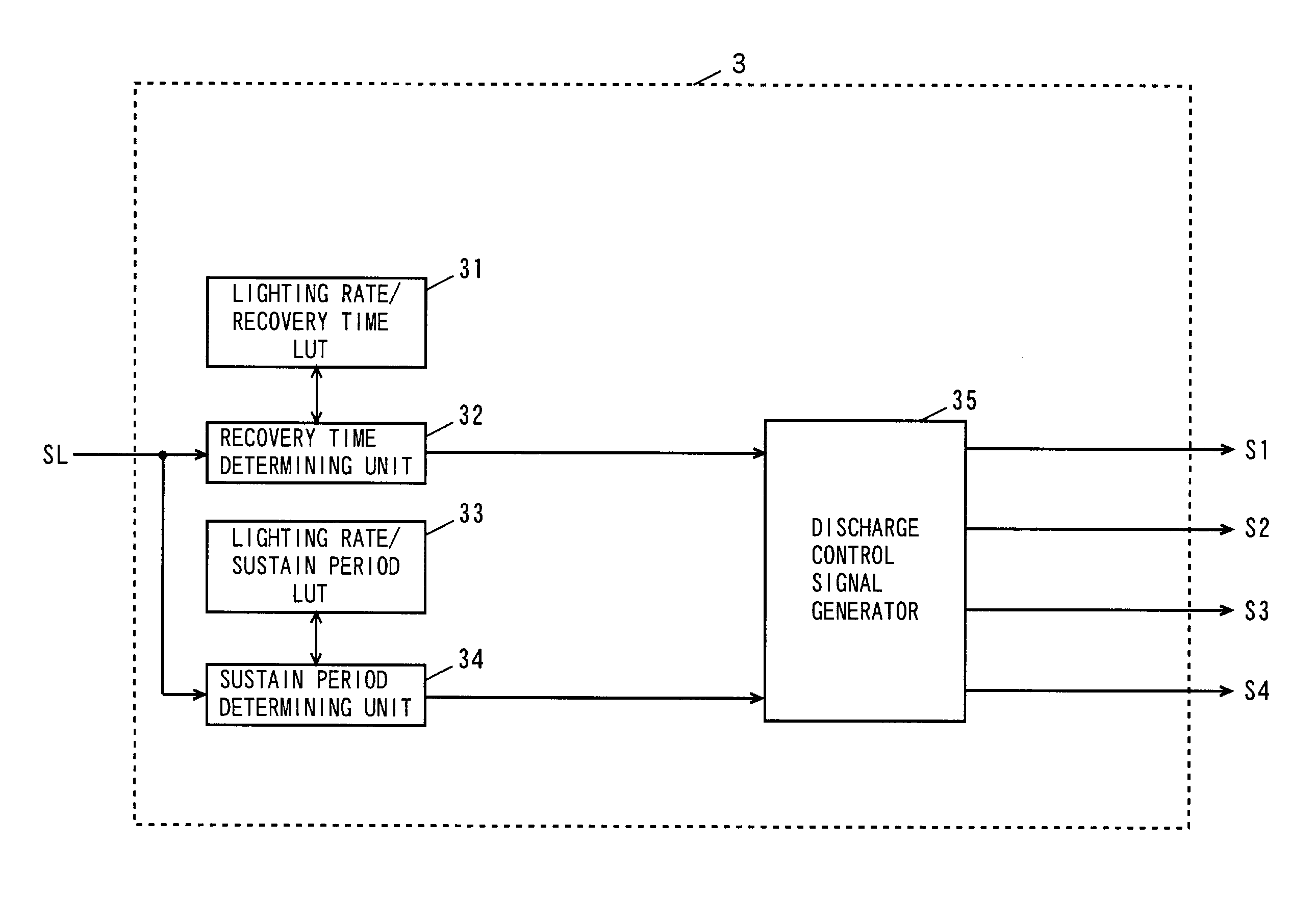
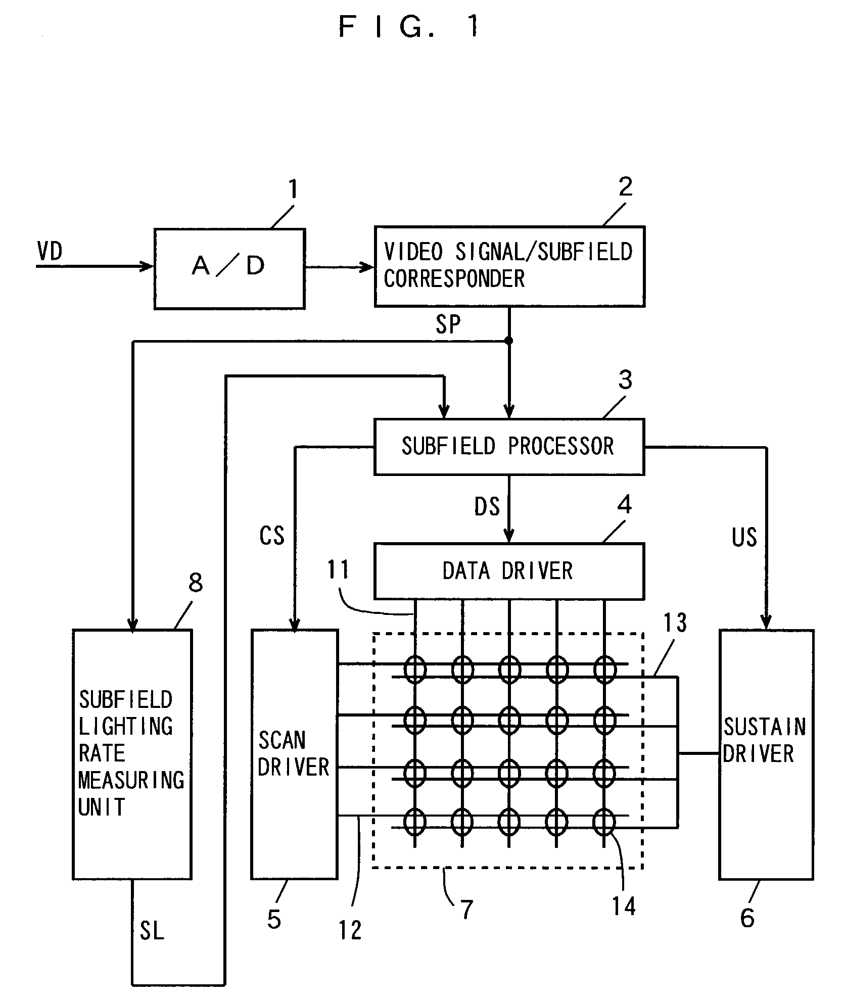
[0113]Description will now be made on an AC type plasma display device as one example of a display device in accordance with the present invention. FIG. 1 is a block diagram showing the structure of a plasma display device according to the present invention.

[0114]The plasma display of FIG. 1 includes an A / D converter (analog-to-digital converter) 1, a video signal / subfield corresponder 2, a subfield processor 3, a data driver 4, a scan driver 5, a sustain driver 6, a PDP (plasma display panel) 7 and a subfield lighting rate measuring unit 8.

[0115]The A / D converter 1 is supplied with a video signal VD. The A / D converter 1 converts an analog video signal VD into digital image data to output the image data to the video signal / subfield corresponder 2. In order to display by dividing one field into a plurality of subfields, the video signal / subfield corresponder 2 produces image data SP for each subfield from image data in one field to output the produced image data SP to the subfield pr...

third embodiment

[0260]In this embodiment, the transistors Q3, Q4, Q7 and Q8, the recovery capacitor Cr, the recovery coils L1 and L2, and the diodes D1 and D2 correspond to recovery means; the subfield processor 3b to control means; the transistors Q7 and Q8, and the recovery coils L2 and L2 to inductance means and variable inductance means; and the transistors Q7 and Q8 to second switch means. The remaining parts are the same as those in the

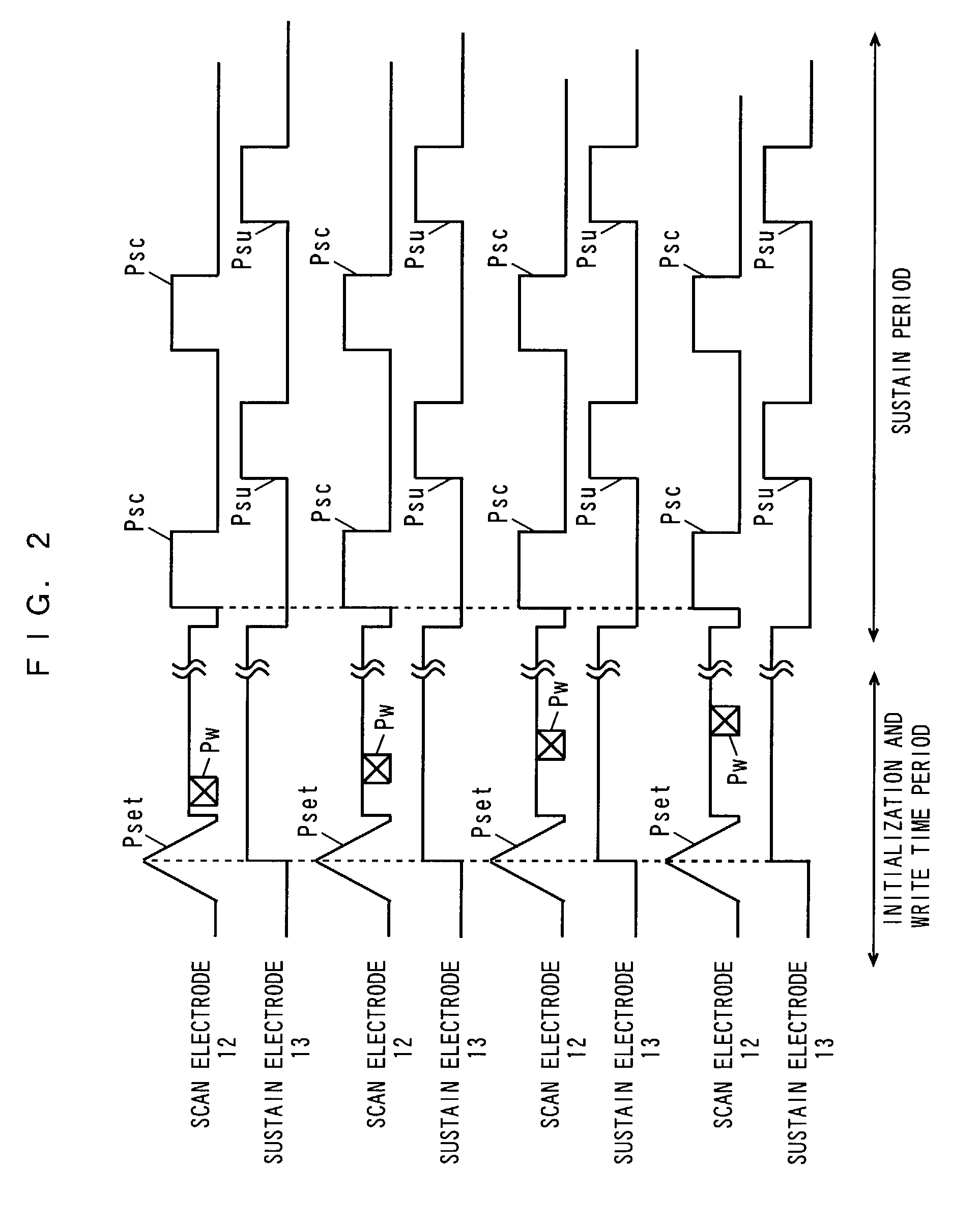
[0261]FIGS. 32 to 35 are timing charts showing operations of the sustain driver 6c of FIG. 31 in the sustain time period. The voltage on the node N1 and the control signals S1 to S5 shown in FIG. 31 are illustrated in FIGS. 32 to 35.

[0262]As shown in FIGS. 32 to 35, in the sustain driver 6c like the third embodiment, a time period TA to be the discharge recovery time, and delay times DT1 and DT2 are controlled depending on the lighting rate, while a time period TC to be the non-discharge recovery time, and delay times DT1 and DT2 are also controlled depending o...

fourth embodiment

[0278]As-shown in FIGS. 39 to 42, in the sustain driver 6d, a time period TA to be the discharge recovery time and delay times DT1 and DT2 are controlled depending on the lighting rate, while a time period TC to be the non-discharge recovery time and delay times DT1 and DT2 are controlled depending on the lighting rate, like the

[0279]As described above, in this embodiment, the lighting rate for each subfield is detected. As the detected lighting rate for each subfield becomes lower, the discharge recovery time, the non-discharge recovery time, the resonance time and the sustain period at the rising and falling of sustain pulses can become longer, resulting in achievement of the same effect as in the first embodiment.

[0280]Furthermore, since the on / off states of the transistors Q9 and Q10 can independently be controlled by the control signals S5 and S6, it is possible to independently control the resonance time at the rising of sustain pulses and that at the falling of the sustain pu...


PUM


Abstract

A subfield lighting rate measuring unit detects a lighting rate for each subfield, and a subfield processor controls a scan driver and a sustain driver so that a recovery time of each sustain pulse, a resonance time of LC resonance and a sustain period become longer as the detected lighting rate for each subfield becomes smaller.

Description

TECHNICAL FIELD[0001]The present invention relates to a display device that selectively discharges a plurality of discharge cells to display an image and a method of driving such a display device.BACKGROUND ART[0002]Plasma display devices using PDPs (plasma display panels) have the advantage capable of being thinner and having larger screens. Such plasma display devices display images by utilizing light emission which occurs in the discharge of discharge cells constituting pixels.[0003]FIG. 47 is a circuit diagram showing the structure of a sustain driver in a conventional plasma display device.[0004]As shown in FIG. 47, a sustain driver 600 includes a recovery capacitor C11, a recovery coil L11, switches SW11, SW12, SW21 and SW22, and diodes D11 and D12.[0005]The switch SW11 is connected between a power supply terminal V11 and a node N11, and the switch SW12 is connected between the node N11 and a ground terminal. The power supply terminal V11 is supplied with a sustain voltage Vsu...

Claims


Application Information

Patent Timeline
IPC IPC(8): G09G3/28
CPCG09G3/2022G09G3/2965G09G3/294G09G2360/16G09G2310/066G09G2330/021
Inventor KIGO, SHIGEOKASAHARA, MITSUHIROMORI, MITSUHIROHASHIGUCHI, JUMPEI
Owner PANASONIC CORP
Why Eureka
Try Eureka