Non-volatile semiconductor memory device and electric device with the same

a semiconductor memory and non-volatile technology, applied in static storage, digital storage, instruments, etc., can solve the problems of reducing power consumption, reducing the power consumption, and large cannon resistance of the nand cell uni

Active Publication Date: 2006-05-23
KIOXIA CORP
View PDF6 Cites 43 Cited by
  • Summary
  • Abstract
  • Description
  • Claims
  • Application Information

AI Technical Summary

Problems solved by technology

However, due to the fact that plural cells are serially connected in the NAND cell unit, the cannel resistance of the NAND cell unit is large, and cell current is small at the data read time.
However, the conventional sense amp scheme for data determining based on the inverter threshold has some problems in viewpoints of lowering the power consumption and increasing the memory capacity in future.
As a result, it becomes difficult to perform a high speed data read operation.
Alternatively, there is a fear that data determination becomes impossible.

Method used


Image

  • Non-volatile semiconductor memory device and electric device with the same
  • Non-volatile semiconductor memory device and electric device with the same
  • Non-volatile semiconductor memory device and electric device with the same

Examples


Embodiment Construction

[0025]Illustrative embodiments of this invention will be explained with reference to the accompanying drawings below.

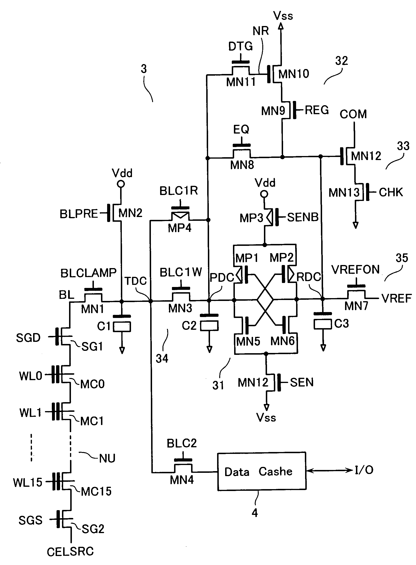
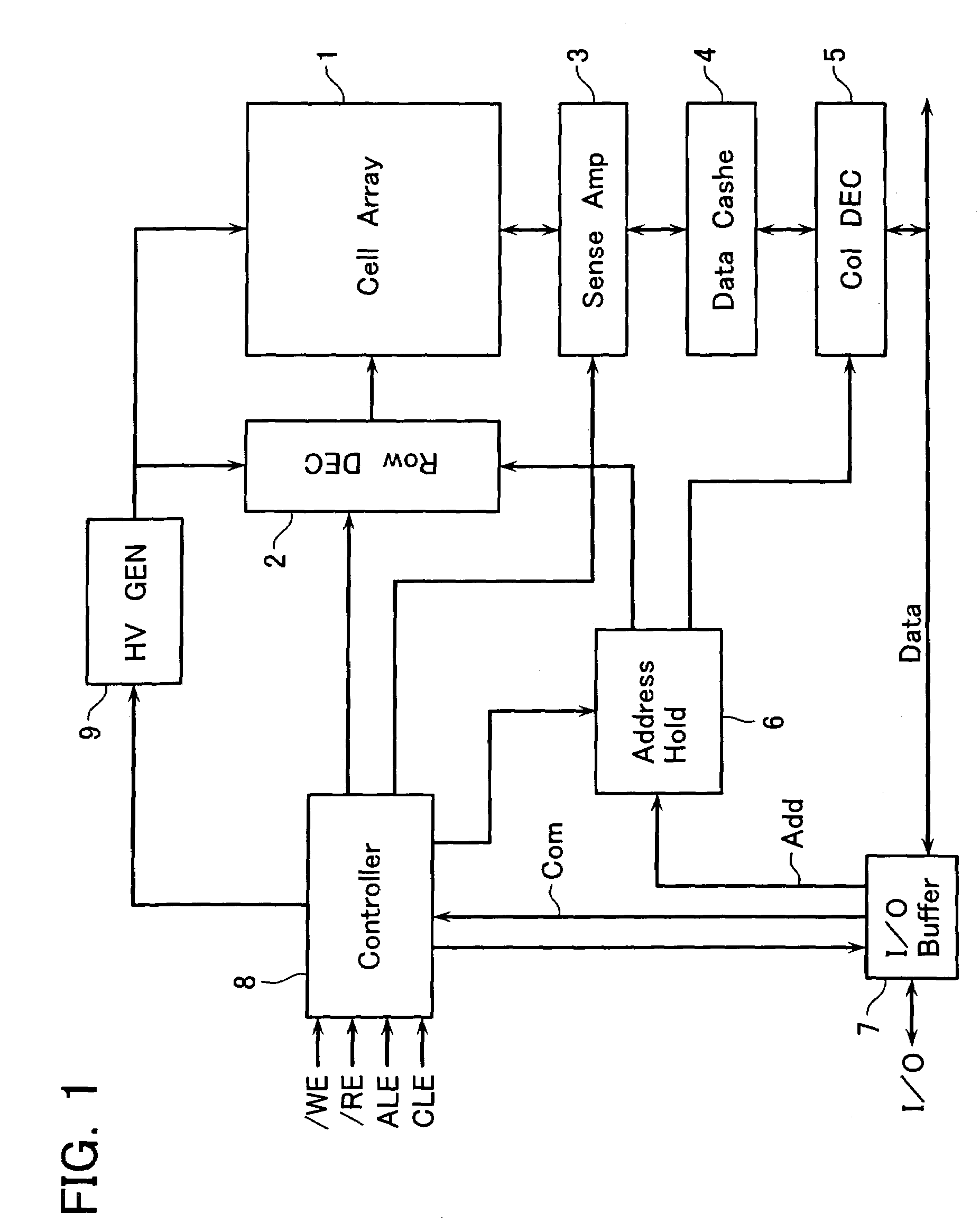
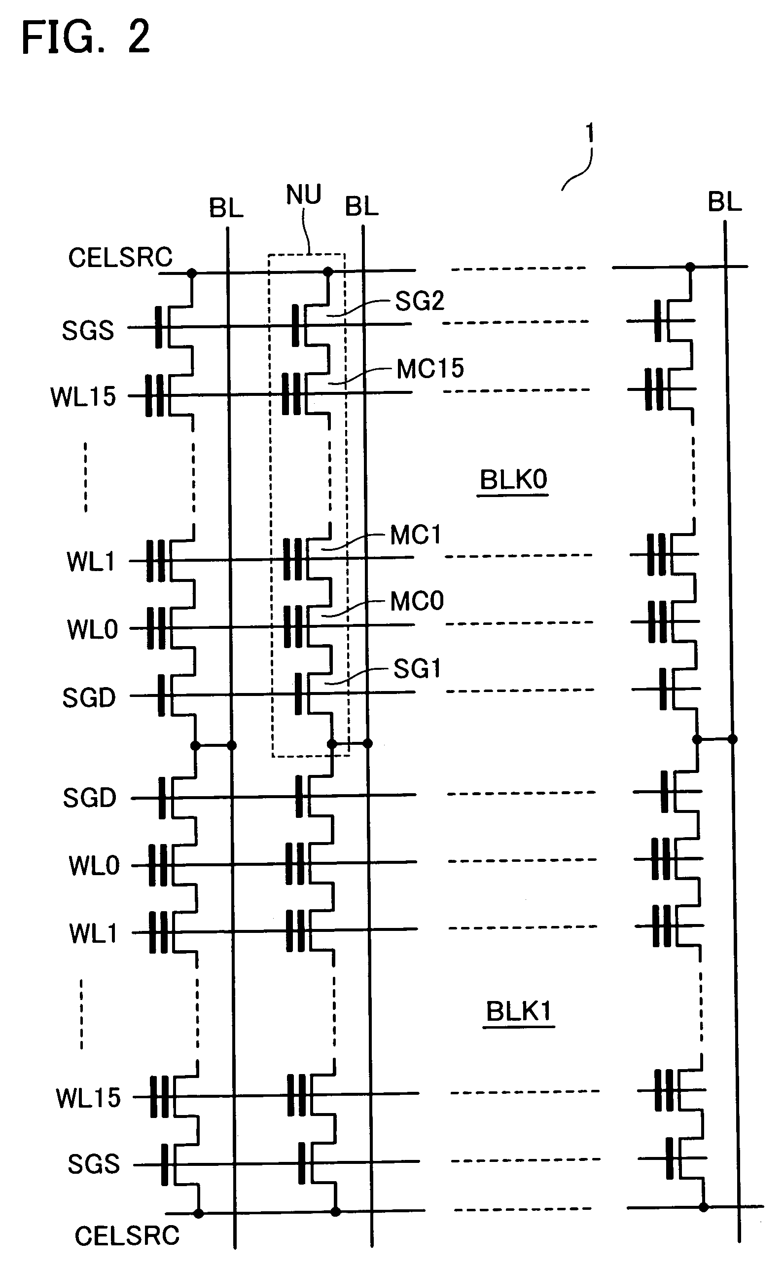
[0026]FIG. 1 shows a circuit architecture of a flash memory according to an embodiment of the present invention. A cell array 1 is, as described later, configured to have a plurality of floating gate type memory cells as being arranged in a matrix manner. A row decoder / word line driver 2 is prepared to select a block and selectively drive word lines and select gate lines of the cell array 1. A sense amplifier circuit 3 serves as a page buffer with sense amplifiers for one page, which is used for bit line data sensing for one page of the cell array 1.

[0027]Data cache (data register) 4 is prepared to temporarily hold read data of the sense amplifier 3 for outputting it outside the chip, and temporarily hold write data supplied from external. One page read data are column-selected by a column decoder (column gate) 5 and output to external I / O terminals via I / O buffer 7. ...


PUM


Abstract

A non-volatile semiconductor memory device includes a cell array in which electrically rewritable and non-volatile memory cells are arranged, and a sense amplifier circuit configured to read and write data in association with the cell array, wherein the sense amplifier circuit includes: differential amplifier having first and second input nodes and configured to amplify a difference voltage between the first and second input nodes; a data transfer circuit configured to selectively connect the first input node to a bit line in the cell array; a reference voltage setting circuit configured to apply a reference voltage to the second input node of the differential amplifier; and a data storing circuit configured to temporarily hold a loaded write data at the first input node of the differential amplifier, and control the reference voltage at the second input node of the differential amplifier in correspondence with the write data held therein.

Description

CROSS-REFERENCE TO RELATED APPLICATION[0001]This application is based on and claims the benefit of priority from the prior Japanese Patent Applications No. 2003-203149, filed on Jul. 29, 2003, and No. 2004-120725, filed on Apr. 15, 2004, the entire contents of which are incorporated herein by reference.BACKGROUND OF THE INVENTION[0002]1. Field of the Invention[0003]This invention relates to a non-volatile semiconductor memory device and an electric device with the same.[0004]2. Description of Related Art[0005]Currently known EEPROMs are formed to have a type of memory cell which stores charge in a floating gate thereof. A NAND type flash memory, which is known as one of these EEPROMs, has a cell array in which NAND cell units are arranged. Each NAND cell unit is configured to have a plurality of memory cells connected in series. In the NAND cell unit, sources and drains are shared between adjacent memory cells. Therefore, NAND type flash memory has a property that it is easy to incr...

Claims


Application Information

Patent Timeline
Patent Type & Authority Patents(United States)
IPC IPC(8): G11C7/02G11C16/04
CPCG11C16/0483
Inventor MAEJIMA, HIROSHIHARA, TAKAHIKO
Owner KIOXIA CORP
Why Eureka
Try Eureka