

Methods for improving sensitivity of CMOS active pixel sensors
a sensitivity improvement and active pixel technology, applied in the field of image sensors, can solve the problems of limited readout rate and dynamic range, active pixel sensor cell b>10///////////////////////////////////
- Summary
- Abstract
- Description
- Claims
- Application Information
AI Technical Summary
Benefits of technology
Problems solved by technology
Method used
Image

Examples
Embodiment Construction
[0027]The invention will be now be described in detail with reference to the accompanying drawings.
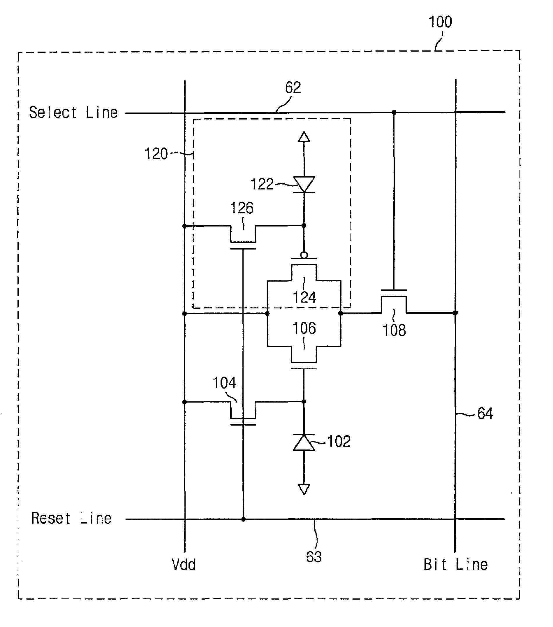
[0028]FIG. 3 is a schematic diagram of an active pixel sensor imaging system according to the present invention. The active pixel sensor imaging system has a row decoder 50, a plurality of differential output circuits 52, a timing controller 54, and an array 90 of active pixel sensors 100. The active pixel sensor array 90 comprises closely spaced active pixel sensors 100 in ten rows and ten columns. The active pixel sensor array 90 is illustrated as a ten-by-ten array for illustrative purposes only and is not meant to be a limitation on the present invention. The active pixel sensor array 90 according to the present invention may be comprised of active pixel sensors 100 in any number of rows and columns, and for many applications the array includes a large number of pixels.
[0029]Each active pixel sensor 100 is capable of converting a detected quantity of light to corresponding electric...
PUM
 Abstract
Description
Claims
Application Information