Semiconductor wafer with ID mark, equipment for and method of manufacturing semiconductor device from them

a technology of semiconductor devices and id marks, which is applied in the field of semiconductor wafers, can solve the problems of relative large space loss of the wafer, markings that may disappear or become unrecognizable, and related arts, however, also have problems

Inactive Publication Date: 2006-06-06
KK TOSHIBA
View PDF23 Cites 38 Cited by
  • Summary
  • Abstract
  • Description
  • Claims
  • Application Information

AI Technical Summary

Benefits of technology

[0357]Additional advantages and modifications of the present invention will readily occur to those skilled in the art. Therefore, the present invention in its broader aspects is not limited to the specific details and representative first to ninth embodiments shown and described herein. Accordingly, various modifications may be made without departing from the spirit or scope of the general inventive concept as defined by the appended claims and their equivalents.

Problems solved by technology

The marking must be visible to workers, and therefore, usually extends from several millimeters to several centimeters causing relatively large space loss on the wafer.
When the marking are formed on the surface of a wafer, the marking may disappear or become unrecognizable due to repetitive deposition and chemical mechanical polishing (CMP) processes carried out on the wafer.
When the marking are formed on the back of a wafer, irregularities in the marking may cause focal errors in a lithography process and will impose the additional work of reversing the wafer in order to see the marking.
The related arts, however, also have problems.
As a result, the processing conditions set for a batch of wafers involve redundancies such as a too long process time, deteriorating productivity and increasing costs.
It is difficult for the related arts to utilize, for example, film thicknesses measured on individual wafers to determine processing conditions applied to the wafers in the next manufacturing process.

Method used


Image

  • Semiconductor wafer with ID mark, equipment for and method of manufacturing semiconductor device from them
  • Semiconductor wafer with ID mark, equipment for and method of manufacturing semiconductor device from them
  • Semiconductor wafer with ID mark, equipment for and method of manufacturing semiconductor device from them

Examples


first embodiment

Modification 4 of First Embodiment

[0145]The method of forming an ID mark according to first embodiment forms an ID mark consisting of dots at the start of a series of semiconductor device manufacturing processes. The method of forming an ID mark may form an ID mark on a wafer during semiconductor device manufacturing processes.

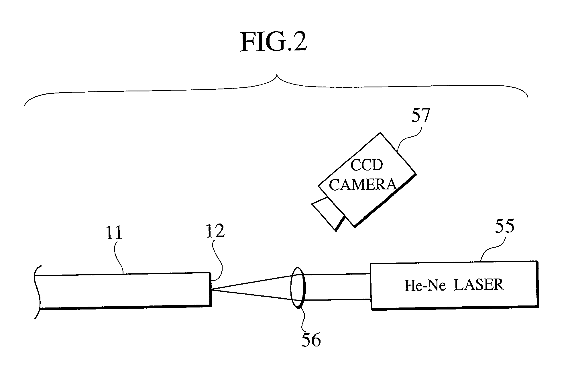
[0146]In FIGS. 4A to 4C, the wafer 16 is etched during a given semiconductor device manufacturing process, to form irregularities each of, for example, 0.2 μm in size and 0.2 μm in height on the surface of the wafer 16. A He—Ne laser beam 18 is emitted onto the surface of the wafer 16 with the He—Ne laser beam 18 focusing above the surface of the wafer 16, to flatten a limited area of the irregularities. A He—Ne laser beam 19 focusing on the surface of the wafer 16 is emitted to form an ID mark consisting of dots in the flattened area.

[0147]In this way, the method of forming an ID mark roughens and flattens an area on a wafer and forms an ID mark consisting of...

second embodiment

Modification 2 of Second Embodiment

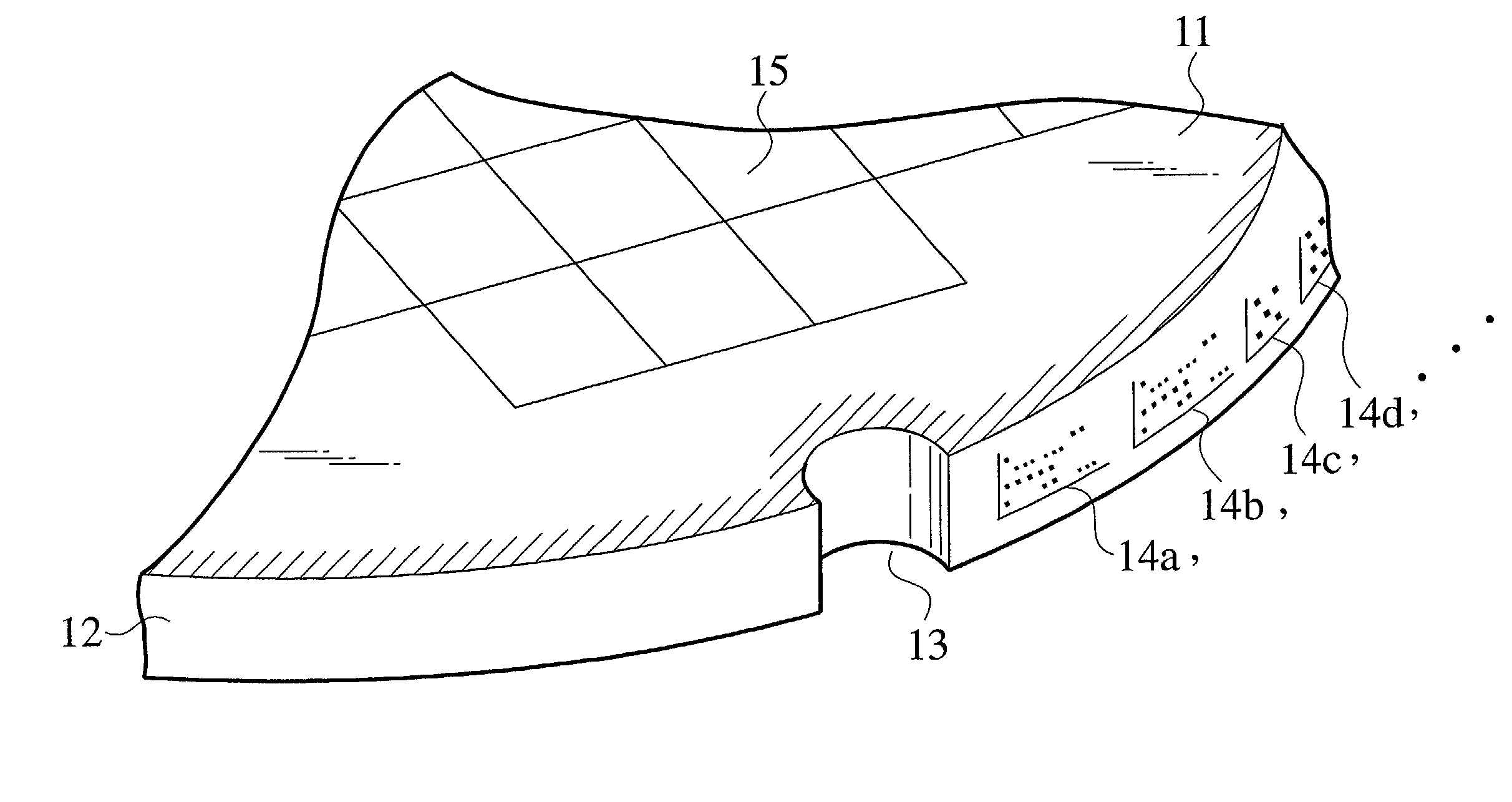
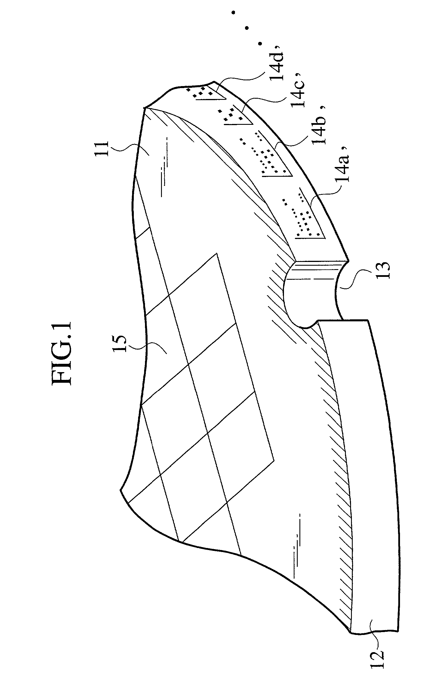
[0160]In FIG. 9, the wafer 31 has a bevel contour 32, which consists of a first bevel contour 32a close to a first principal plane 29 of the wafer 31 and a second bevel contour 32b close to a second principal plane 30 of the wafer 31 opposite to the first principal plane 29. ID marks 33a and 33b having the same data are formed on the first and second bevel contours 32a and 32b, respectively. Namely, the modification 2 forms the identical ID marks 33a and 33b on the surface and back peripheral parts of the wafer 31, respectively. The first principal plane 29 is the surface of the wafer 31 where semiconductor device is formed, and the second principal plane 30 is the back of the wafer 31.

[0161]The modification 2 divides a bevel contour of a wafer into a plurality of areas and forms identical ID marks in the divided bevel contours, respectively. Even if the ID mark 33a on the surface 29 of the wafer 31 is erased during a CMP process, the ID mark 33b o...

third embodiment

Modification of Third Embodiment

[0171]A modification of the third embodiment forms a wafer-maker ID mark (37 in FIG. 10) and a device-maker ID mark (38 in FIG. 10) on the surface and back of a wafer, respectively, to provide the same effect as the third embodiment. In particular, the modification forms the wafer-maker ID mark on the back of a bevel contour of the wafer and the device-maker ID mark on the surface of the bevel contour, to provide a new effect.

[0172]Recent semiconductor device manufacturing lines involve many CMP processes. The CMP processes easily erase ID marks made on the surface of a bevel contour of a wafer. Once an ID mark is erased, it is difficult to make the same mark again because data contained in the erased ID mark is unreadable.

[0173]To cope with this problem, the modification forms a wafer-maker ID mark on the back of a bevel contour of a wafer so that the ID mark is difficult to erase, and a device-maker ID mark on the surface of the bevel contour. At th...


PUM


Abstract

A semiconductor wafer has a bevel contour formed along the periphery thereof, products formed on the wafer, and an ID mark formed on the bevel contour. The ID mark shows at least the properties, manufacturing conditions, and test results of the products.

Description

CROSS REFERENCE TO RELATED APPLICATIONS[0001]This application is based upon and claims the benefit of priority from the prior Japanese Patent Applications No. P2001-80452 filed on Mar. 21, 2001 and No. P2001-345984 filed on Nov. 12, 2001, the entire contents of which are incorporated herein by reference.BACKGROUND OF THE INVENTION[0002]1. Field of the Invention[0003]The present invention relates to a semiconductor wafer having an ID mark on the periphery thereof and a method of manufacturing such a semiconductor wafer. The present invention also relates to an equipment for and a method of manufacturing semiconductor device from such a semiconductor wafer.[0004]2. Description of the Related Art[0005]Semiconductor device manufacturing involves several hundreds of processes each of which needs different conditions that must be strictly managed. Management of the process conditions of wafers employs markings made on the wafers. These markings consist of, for example, numerals, character...

Claims


Application Information

Patent Timeline
Patent Type & Authority Patents(United States)
IPC IPC(8): H01L29/06H01L21/02H01L23/544
CPCH01L23/544H01L2223/54406H01L2223/54413H01L2223/54433H01L2223/54493H01L2924/0002Y10S438/974H01L2924/00H01L21/02
Inventor ARIKADO, TSUNETOSHIIWASE, MASAONADAHARA, SOICHIUDO, YUSOUSHIKU, YUKIHIRONITTA, SHINICHIMIYASHITA, MORIYASUGAMOTO, JUNJIYAMADA, HIROAKINAGANO, HAJIMETANZAWA, KATSUJIROMATSUSHITA, HIROSHITSUCHIYA, NORIHIKOOKUMURA, KATSUYA
Owner KK TOSHIBA
Why Eureka
Try Eureka