Noise filter for an integrated circuit

a noise filter and integrated circuit technology, applied in the field of noise filters, can solve the problems of insufficient noise filters of the prior art, inability to meet the needs of deep sub-micron lsi, and failure of the lsi to function properly, so as to prevent the lsi from the malfunction

Inactive Publication Date: 2006-06-06
WINBOND ELECTRONICS CORP
View PDF21 Cites 16 Cited by
  • Summary
  • Abstract
  • Description
  • Claims
  • Application Information

AI Technical Summary

Benefits of technology

[0010]The object of the present invention is to provide a noise filter to prevent an LSI from the mal-function caused by the external EMI.
[0012]Another object of the present invention is to provide a noise filter that can operate in high frequency.

Problems solved by technology

It is known that the external Electro-Magnetic noise from a motor or a breaker causes a spike noise on the power lines and signals of the LSI will cause functional failures in the LSI.
However if the following conditions happen, the noise filter of the prior art is not good enough anymore.
(2) High resistance poly-silicon is not available in the deep sub-micron LSI.

Method used


Image

  • Noise filter for an integrated circuit
  • Noise filter for an integrated circuit
  • Noise filter for an integrated circuit

Examples


Embodiment Construction

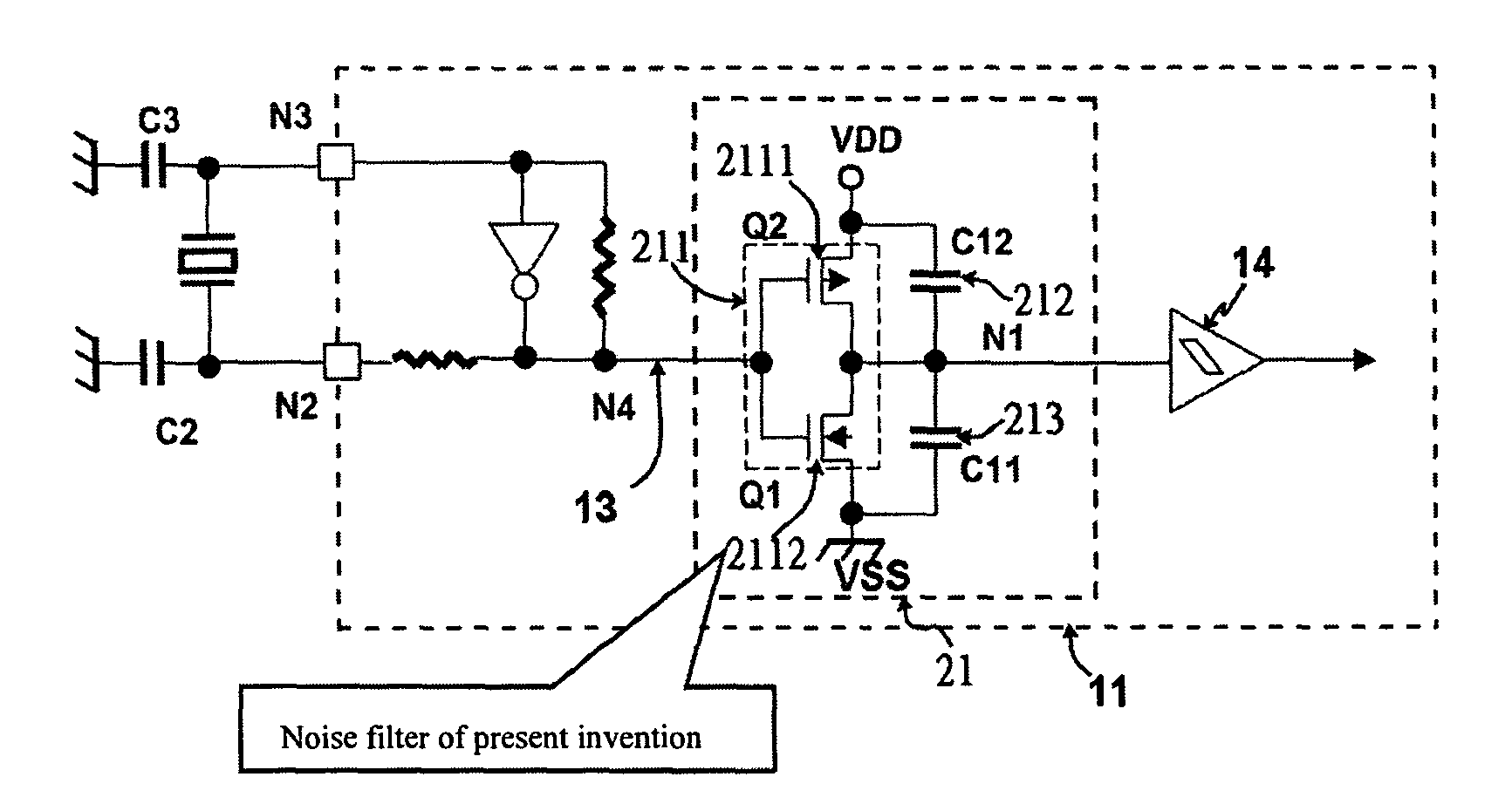
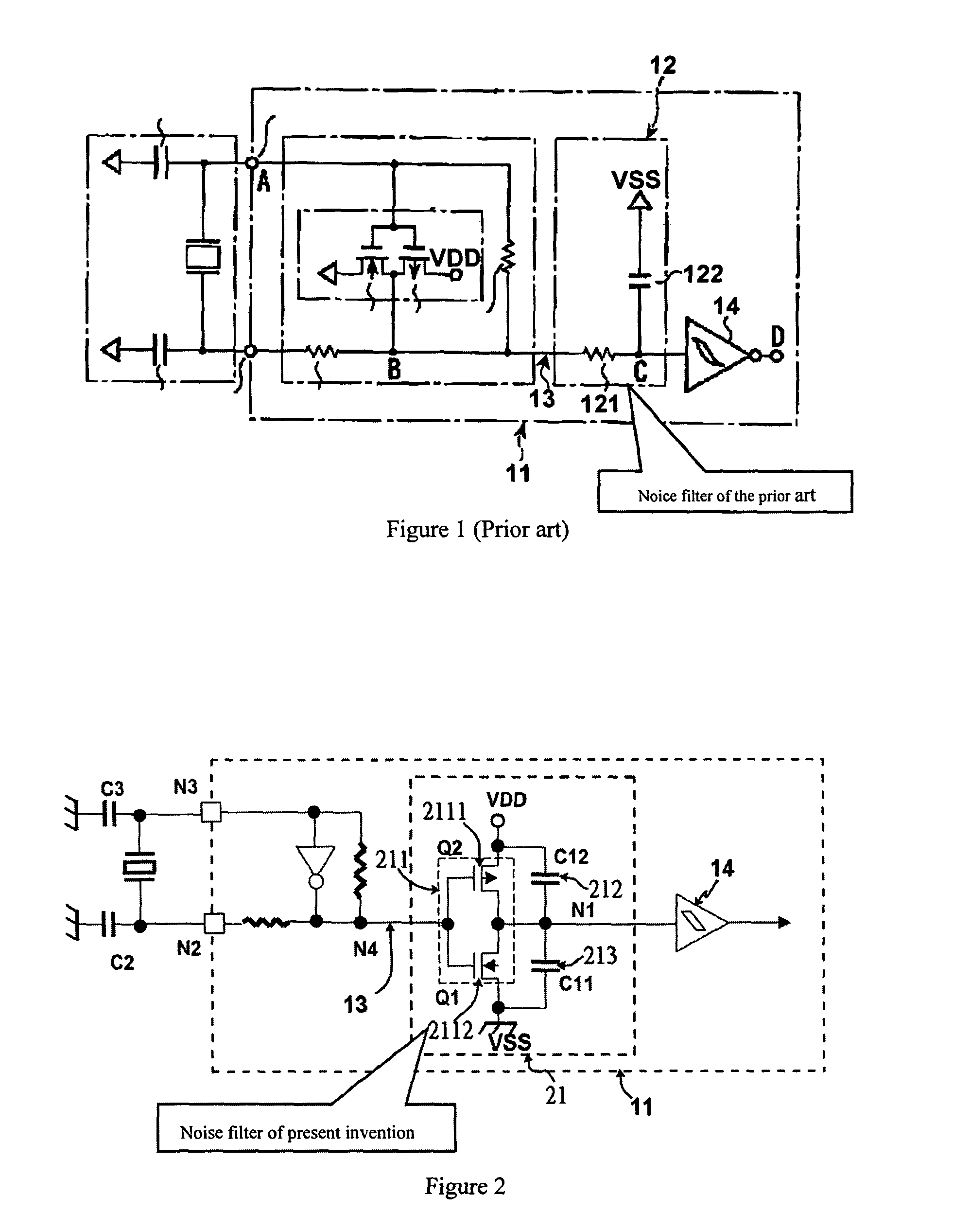
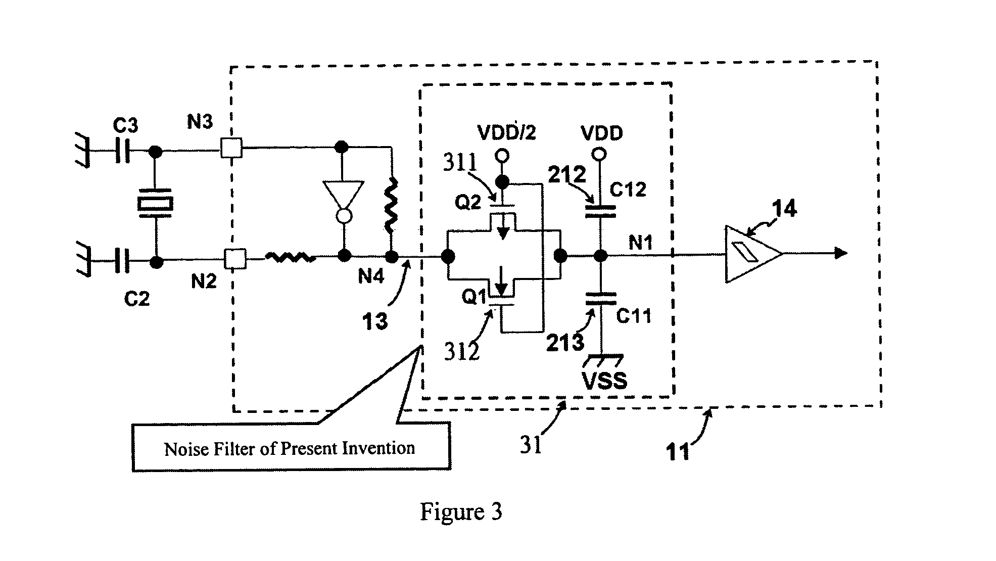
[0037]The new noise filter 21 shown in FIG. 2 consists with one CMOS inverter 211 and two capacitors 212,213. The input gate of the inverter 211 is coupled with the input pad 13, and the output of the inverter 211 is coupled with the input gate of the input buffer 14. The first capacitors 212 is inserted between the output N1 of the inverter 211 and the VDD of the LSI and the 2nd capacitor 213 is inserted between the output N1 of the inverter 211 and the VSS of the LSI.

[0038]By using the present invention, we can overcome the problems of the prior arts listed in the previous page as explained below.

[0039](1) In case a noise is applied between VDD and VSS, the input voltage of the input buffer which is stored in the two capacitors, changes according to the voltage between VDD and VSS because the voltage between VDD and VSS is divided by the two capacitors 212,213. The threshold voltage of the input buffer 14 also changes according to the voltage between VDD and VSS. Assuming the thre...


PUM


Abstract

A noise filter for an integrated circuit is proposed. The noise filter comprises a CMOS inverter and two capacitors. The input of the CMOS inverter is coupled with an input pad of the integrated circuit and the output of the CMOS inverter is coupled with an input buffer. The first capacitor is inserted between the output of the CMOS inverter and a first voltage source and the second capacitor is inserted between the output of the CMOS inverter and a second voltage source. A transfer gate may be in stead of the CMOS inverter.

Description

FIELD OF THE INVENTION[0001]The present invention is relative to a noise filter, and more particularly to prevent a LSI (Large-Scale integration) from the malfunction caused by the external EMI (Electro-Magetic Interference).BACKGROUND OF THE INVENTION[0002]It is known that the external Electro-Magnetic noise from a motor or a breaker causes a spike noise on the power lines and signals of the LSI will cause functional failures in the LSI.[0003]To prevent this problem, a noise filter has been inserted between the input pad and the input gate of the input buffer as shown in FIG. 1. This noise filter consists of a resistor and capacitor. The resistor connects the input pad and the input gate of the input buffer. The capacitor is inserted between the input gate and the ground of the LSI.[0004]If the noise pulse is applied between the input pad and the ground line, the noise pulse is absorbed by the noise filter and the noise is not detected by the input buffer.[0005]As far as the voltag...

Claims


Application Information

Patent Timeline
Patent Type & Authority Patents(United States)
IPC IPC(8): H04B1/10H03B1/00H03H11/46H03H19/00
CPCH03H19/008
Inventor KOIKE, HIDEHARU
Owner WINBOND ELECTRONICS CORP
Why Eureka
Try Eureka