Semiconductor integrated circuit device having a test function

a technology of integrated circuit and test function, which is applied in the direction of electronic circuit testing, digital storage, instruments, etc., can solve the problems of lsi devices, test cost remarkably increased, and the inability to request chips without chips

Inactive Publication Date: 2006-06-06
KK TOSHIBA
View PDF3 Cites 34 Cited by
  • Summary
  • Abstract
  • Description
  • Claims
  • Application Information

AI Technical Summary

Benefits of technology

[0041]FIG. 12 is a flowchart to explain the test process carried o

Problems solved by technology

Memory circuits have large capacities, and thereby, it is impossible to request chips having no defect at all.
In this case, the test cost remarkably increases as compared with logic LSI devices embedding no memory or memory embedded logic LSI devices having no redundancy function.
(1) Test devices, such as test boards and probe cards for carrying out the test, must be prepared;

Method used


Image

  • Semiconductor integrated circuit device having a test function
  • Semiconductor integrated circuit device having a test function
  • Semiconductor integrated circuit device having a test function

Examples


Embodiment Construction

[0043]An embodiment of the present invention will be described below with reference to the accompanying drawings.

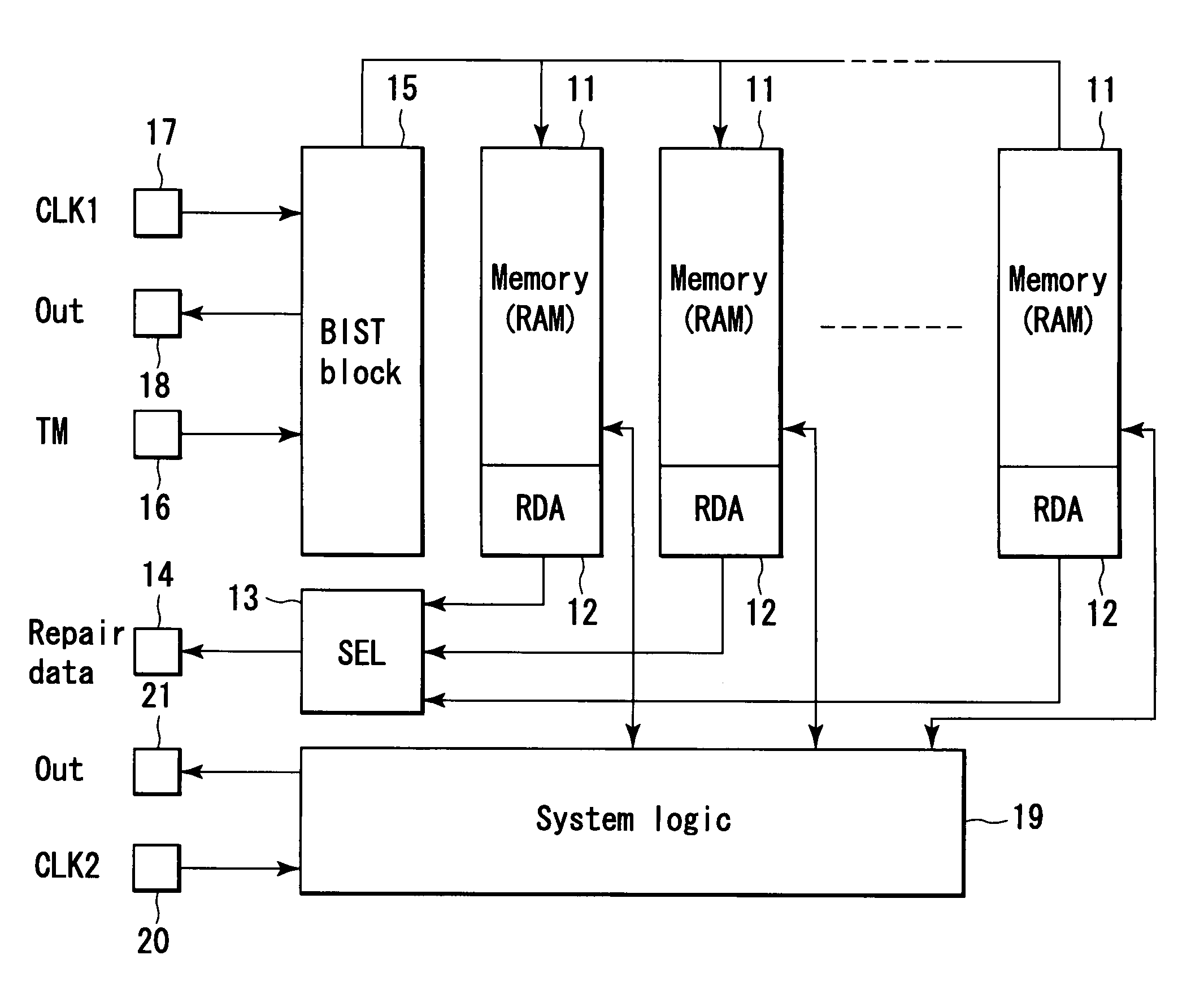
[0044]FIG. 4 is a block diagram showing the entire configuration of a memory embedded logic LSI device. The LSI device is provided with a plurality of memory collars 11 each having a RAM as memory. The memory collars 11 each include a memory cell array and peripheral circuits such as row decoder and column decoder. The memory collar 11 carries out a test to determine whether or not memory cells included in the memory cell array have failed. If a fail cell exists, the memory collar 11 has a redundancy function of generating a fail cell address and replacing it with a redundancy spare cell. A repair data analyzer (RDA) 12 included in each memory collar 11 generates the fail cell address. A selector circuit (SEL) 13 selects the fail cell address generated by the repair data analyzer 12 included in each memory collar 11. Thereafter, the fail cell address is outputted as repai...


PUM


Abstract

A semiconductor memory device includes a memory collar, a repair data analyzer, a BIST block, and a system logic. The memory collar includes a memory cell and a spare cell and have a redundancy function of replacing fail memory cell with the spare cell if fail memory cell exists. The repair data analyzer determines whether or not memory cell included in the memory collar is defective, and generates fail address corresponding to the memory cell determined as being defective. The BIST block operates in synchrony with a first clock signal inputted to a first clock signal terminal in a test operation mode, and controls the operation of the memory collar. The system logic operates in synchrony with a second clock signal inputted to a second clock signal terminal in the test operation mode.

Description

CROSS-REFERENCE TO RELATED APPLICATIONS[0001]This application is based upon and claims the benefit of priority from prior Japanese Patent Application No. 2003-123740, filed Apr. 28, 2003, the entire contents of which are incorporated herein by reference.BACKGROUND OF THE INVENTION[0002]1. Field of the Invention[0003]The present invention relates to a memory embedded logic LSI device. In particular, the present invention relates to a semiconductor integrated circuit device in which a test is carried out with respect to memory and logic circuits.[0004]2. Description of the Related Art[0005]Conventionally, logic LSI and memory LSI have been used separately from each other as the need arises. However, the semiconductor micro-fabrication technique has recently advanced, and thereby, both logic LSI and memory LSI are assembled into one chip. In recent years, product development has been frequently made in memory embedded logic LSI devices embedding logic and memory circuits in one chip. F...

Claims


Application Information

Patent Timeline
IPC IPC(8): G11C7/00G01R31/28G11C11/22G11C11/401G11C11/413G11C29/04G11C29/12G11C29/44
CPCG11C29/4401G11C29/44
Inventor SHIMIZU, MITSURUYAMAMOTO, TETSUYA
Owner KK TOSHIBA
Why Eureka
Try Eureka