

High speed vertical cavity surface emitting laser device (VCSEL) with low parasitic capacitance
a laser device and low parasitic capacitance technology, applied in lasers, laser details, electrical apparatus, etc., can solve the problems of limited maximum modulation speed of vcsels, signal distortion, bonding failure, etc., and achieve low parasitic packaging, reliable fabrication and packaging procedures, and reduce electrical parasitics
- Summary
- Abstract
- Description
- Claims
- Application Information
AI Technical Summary
Benefits of technology
Problems solved by technology
Method used
Image

Examples
first embodiment
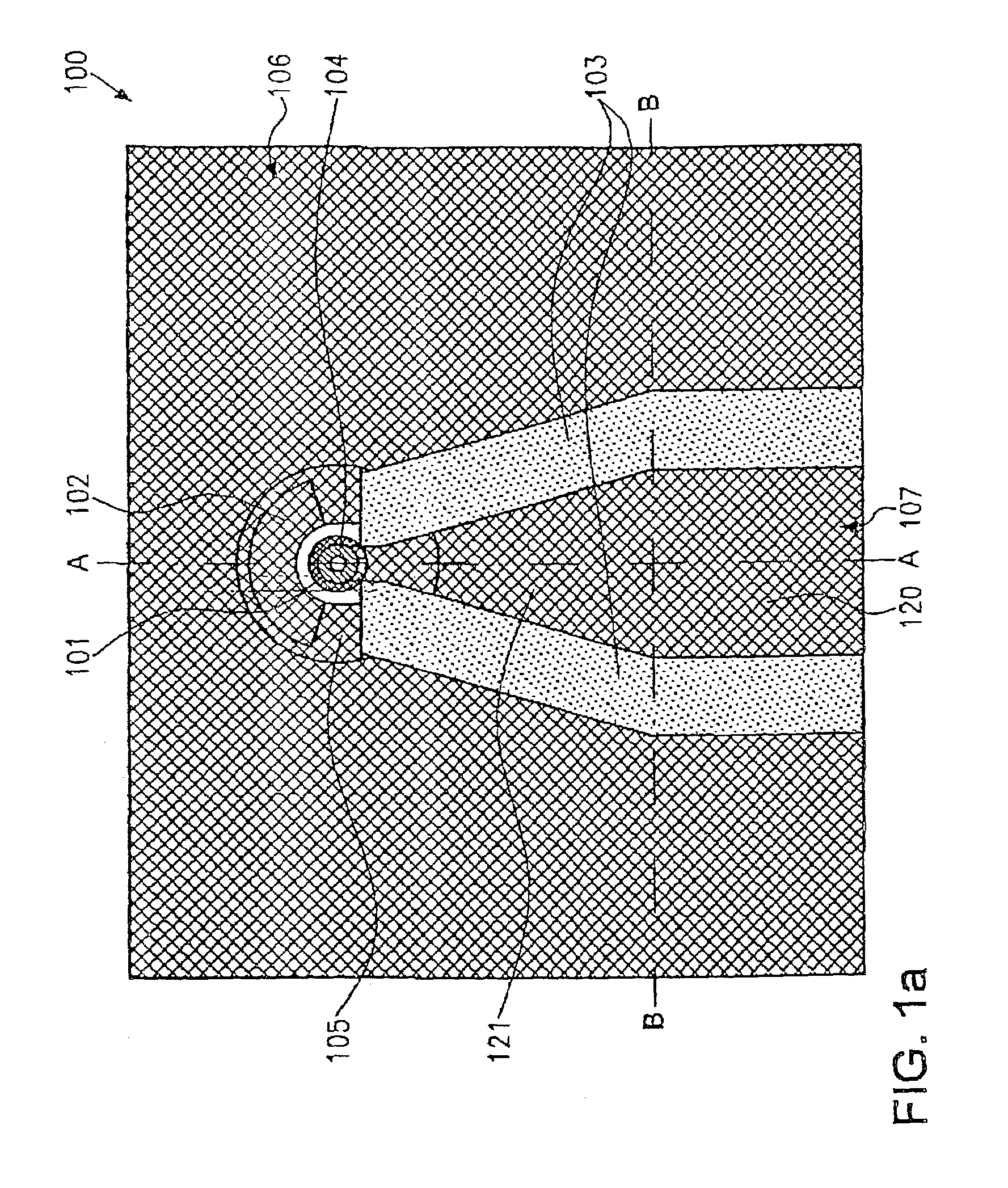
[0074]With the present invention, illustrated in FIG. 1a, there are three distinguishing regions within the first trench 105. The first region is covered by a conductive material which connects the ring-shaped electrode 104 on top of the mesa 101 with the rectangular bond pad 120 and is part of the second contact portion107. The second region of the first trench 105 is part of the second trenches 103. The third region is part of the first contact portion 106 which connects electrically the first distributed Bragg reflector. The third region of the first trench 105 is at least partly covered by the second layer of conductive material 102.
[0075]With the first embodiment in FIG. 1a the third layer of conductive material covers the third part of the first trench 105. The third layer of conductive material is spread over the rest of the chip surface apart from the mesa 101, the second trenches 103 and the second contact portion 107 and connects electrically a first bond pad anywhere on t...
second embodiment
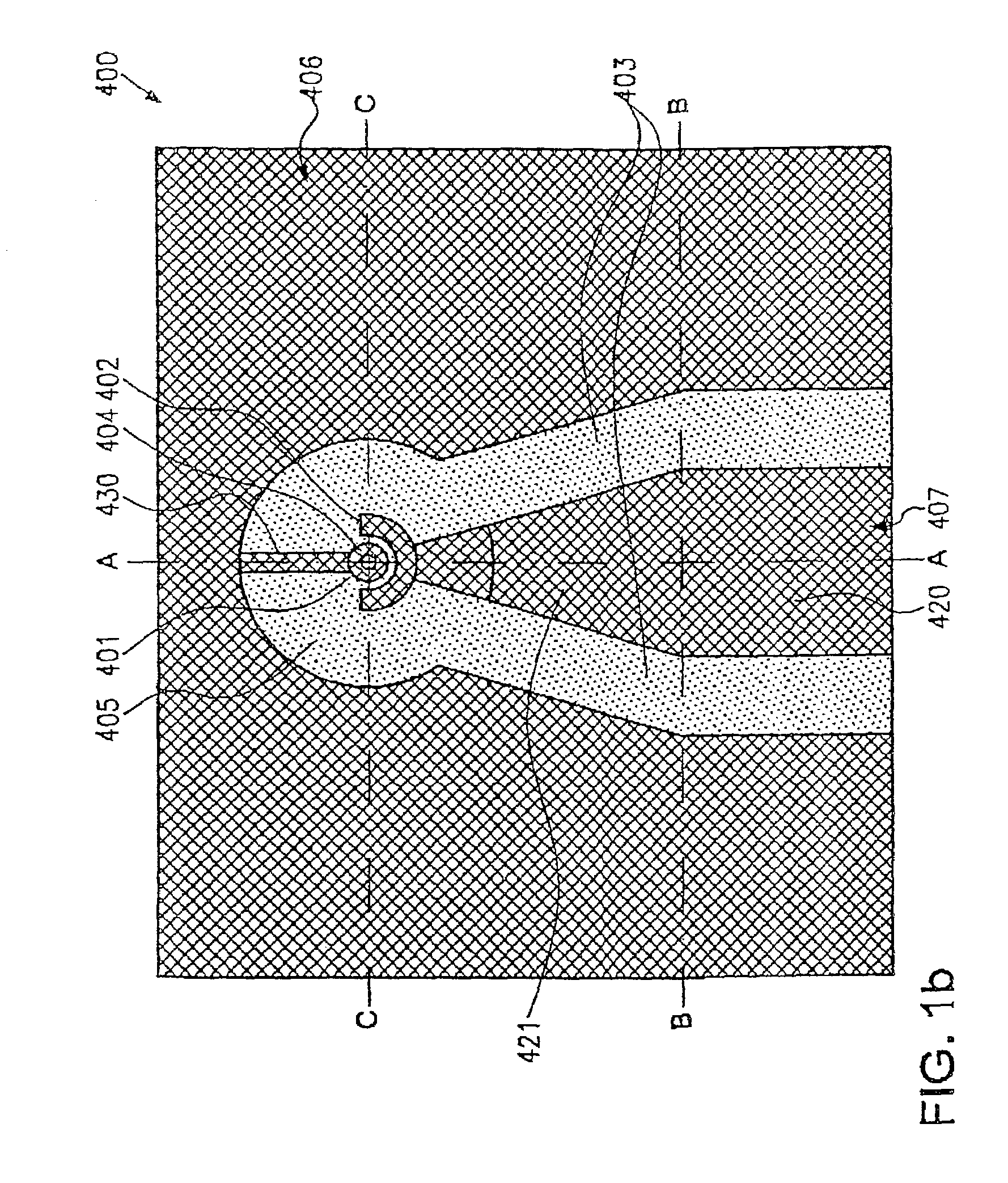
[0077]In the case of the present invention, exemplified in FIG. 1b, the first trench 405 can also be separated into three distinguishing regions. However, the regions are located at different positions. Here, the first region covered by a conductive material is on the opposite side of the mesa and connects the ring-shaped electrode 404 on top of the mesa 401 with the bond pads of the first contact portion 406. The second region of the first trench 405 almost surrounds the mesa and is part of the second trenches 403. Here, the third region is part of the second contact portion 407 and connects the first distributed Bragg reflector. The third region of the first trench 405 is at least partly covered by the second layer of conductive material 402.
[0078]In the context of the latter embodiment (FIG. 1b) the first contact portion 406 is similarly defined as before and comprises the first bondpads and the conductive strip connecting these bondpads to the ring-shaped electrode 404 across th...
PUM
 Abstract
Description
Claims
Application Information