
Negative photoresist compositions for the formation of thick films, photoresist films and methods of forming bumps using the same

a technology of photoresist composition and thick film, applied in the direction of photosensitive materials, instruments, photomechanical equipment, etc., can solve the problems of deterioration of compatibility or stability in preservation, required plating resistance, etc., and achieve satisfactory plating resistance and high sensitivity

Inactive Publication Date: 2006-06-20
TOKYO OHKA KOGYO CO LTD
View PDF18 Cites 15 Cited by
  • Summary
  • Abstract
  • Description
  • Claims
  • Application Information

AI Technical Summary

Benefits of technology

[0009]Accordingly, an object of the present invention is to provide a negative photoresist composition for the formation of thick films, which has high sensitivity and satisfactory plating resistance, is suitable for the formation of thick films and is advantageous as a material for the formation of bumps, as well as to provide a photoresist film and a method of forming bumps using the photoresist film.
[0019]Thus, the present invention provides a negative photoresist composition for the formation of thick films, which has high sensitivity and satisfactory plating resistance, is suitable for the formation of thick films and is advantageous as a material for the formation of bumps, as well as a photoresist film and a method of forming bumps using the photoresist film.

Problems solved by technology

However, large amounts of reaction initiators may deteriorate compatibility or stability in preservation.
However, when thick films are formed using these chemically amplified resists, the resulting thick films invite cracking and do not exhibit required plating resistance.

Method used


Image

  • Negative photoresist compositions for the formation of thick films, photoresist films and methods of forming bumps using the same
  • Negative photoresist compositions for the formation of thick films, photoresist films and methods of forming bumps using the same
  • Negative photoresist compositions for the formation of thick films, photoresist films and methods of forming bumps using the same

Examples


synthesis example 1

Synthesis of Alkali-soluble Novolak Resin (A)

[0069]Sixty parts of m-cresol was added to forty parts of p-cresol, the resulting mixture was condensed with formaldehyde (as formalin) using an oxalic acid catalyst according to a conventional procedure and thereby yielded a cresol novolak resin. Low molecular weight fractions of the resin were removed by fractionation to yield an alkali-soluble novolak resin having a weight average molecular weight of 15000 (novolak resin A).

synthesis example 2

Synthesis of Alkali-Soluble Acrylic Resin (B)

[0070]The inside of a flask equipped with a stirrer, reflux condenser, thermometer and dropping funnel was replaced by nitrogen gas, and 200 g of propylene glycol methyl ether acetate as a solvent was placed in the flask, followed by stirring. Thereafter, the temperature of the solvent was raised to 80° C. Into the dropping funnel, 0.5 g of 2,2′-azobisisobutyronitrile as a polymerization initiator (available from Wako Pure Chemical Industries, Ltd. under the trade name of V-65), 130 g of 2-methoxyethyl acrylate, 50.0 g of benzyl methacrylate and 20.0 g of acrylic acid were charged, followed by stirring until the polymerization initiator dissolved. The resulting solution was uniformly dropped into the flask over 3 hours and was allowed to react at 80° C. for further five hours. The reaction mixture was then cooled to room temperature and thereby yielded an acrylic resin (alkali-soluble acrylic resin B).

example 1

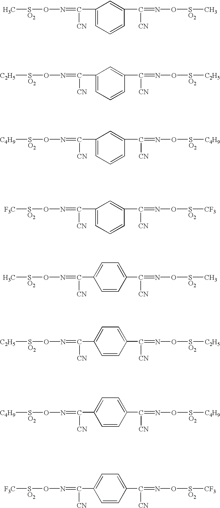
[0071]In 150 parts of propylene glycol methyl ether acetate were dissolved 75 parts of the novolak resin A, 15 parts of the alkali-soluble acrylic resin B, 10 parts of hexamethoxymethylated melamine (available from Sanwa Chemical Co., Ltd. under the trade name of Nikalac Mw-100) as a crosslinking agent (C) and 0.3 part of an acid generator (D) represented by the following formula, the resulting solution was filtrated using a membrane filter having a pore size of 1.0 μm and thereby yielded a negative photoresist composition. The properties of this composition were determined according to procedures mentioned later. The results are shown in Table 1.

[0072]


PUM

PropertyMeasurementUnit
thicknessaaaaaaaaaa
heightaaaaaaaaaa
thicknessaaaaaaaaaa

Abstract

A negative photoresist composition is used for the formation of thick films and includes (A) a novolak resin, (B) a plasticizer, (C) a crosslinking agent and (D) an acid generator. The composition is applied onto a substrate and thereby yields a photoresist film 5 to 100 μm thick. Likewise, the composition is applied onto a substrate of an electronic part, is patterned, is plated and thereby yields a bump.

Description

BACKGROUND OF THE INVENTION[0001]1. Field of the Invention[0002]The present invention relates to a negative photoresist composition for use in the formation of thick films, as well as to a photoresist film and a method of forming bumps using the photoresist film. Specifically, the invention relates to an alkali-developable negative photoresist composition for the formation of thick films which is suitable for photofabrication such as bump formation, wiring, interlayer insulating film formation, circuit protective film formation and processing and manufacture of precision parts, carried out when circuit substrates are manufactured and semiconductors and electronic parts are packaged on the circuit substrates.[0003]2. Description of the Related Art[0004]The photofabrication is a generic term for techniques in which a photosensitive resin composition is coated on the surfaces of process articles and the coating films formed are patterned by photolithography, followed by chemical etchin...

Claims


Application Information

Patent Timeline
Patent Type & Authority Patents(United States)
IPC IPC(8): G03F7/038G03F7/40G03F7/11G03F7/023G03F7/027G03F7/004
CPCG03F7/0045G03F7/038G03F7/0382Y10S430/113Y10S430/111
Inventor SAITO, KOJIMISUMI, KOUICHIOKUI, TOSHIKIKOMANO, HIROSHI
Owner TOKYO OHKA KOGYO CO LTD
Learn More