Multi-layer overlay measurement and correction technique for IC manufacturing

a multi-layer overlay and measurement and correction technology, applied in semiconductor/solid-state device testing/measurement, instruments, photomechanical equipment, etc., can solve problems such as affecting chip reliability, compromising the performance of a completed ic, and compromitting the performance of electrically active regions, so as to facilitate the facilitate measurement and correction of overlay errors, and mitigate repetitive occurrences of overlay errors

Inactive Publication Date: 2006-06-20
GLOBALFOUNDRIES INC
View PDF16 Cites 49 Cited by
  • Summary
  • Abstract
  • Description
  • Claims
  • Application Information

AI Technical Summary

Benefits of technology

[0010]The present invention facilitates measurement and correction of overlay error between multiple layers of an integrated circuit on a wafer, thus mitigating repetitive occurrences of overlay error over a plurality of layers. Furthermore, the present invention allows for design specifications relating to overlay between multiple layers within a wafer. Overlay target(s) that represent overlay between multiple layers are provided to enable measurement of overlay between such layers. The overlay targets can be of a box-in-box structure, frame-in frame structure, segmented frame structure, grating structure overlay targets or other suitable periodic structure overlay marks, or any other suitable structure that enables representation of overlay between more than two layers of a wafer. The overlay target(s) can be analyzed to determine an existing amount of overlay error between adjacent and non-adjacent layers on a wafer. For example, optical microscopy, scatterometry, scanning electron microscopy, and Fourier transform infrared scatterometry can be employed in connection with measuring overlay error between multiple layers. Furthermore, when utilizing periodic structure overlay marks, overlay error can be calculated via determining pitch of such overlay marks, which can be user-defined or measured in real time.
[0011]Measurements relating to overlay error between multiple layers can be utilized to correct such overlay error. For instance, a control system can be provided, wherein such control system can utilize the overlay error measurements as feedback and / or feed-forward data, thus facilitating correction of overlay error between multiple layers of a wafer via controlling fabrication component(s) utilized in connection with a fabrication process. For example, temperature within a process chamber can be manipulated to facilitate correction of overlay error to design specifications between multiple layers.

Problems solved by technology

If layers are not aligned within acceptable tolerances, overlay errors can compromise performance of electrically active regions and adversely affecting chip reliability.
However, in ICs with multiple layers, repeated overlay error(s) (even slight error(s)) between multiple layers can result in compromised performance of a completed IC.
If fabrication device(s) and / or process(es) causing such overlay error 200 are not modified to mitigate such overlay errors, a large aggregated discrepancy results between non-adjacent devices in non-adjacent layers.
Such substantial rotation and displacement between layers and / or devices can compromise IC performance.

Method used


Image

  • Multi-layer overlay measurement and correction technique for IC manufacturing
  • Multi-layer overlay measurement and correction technique for IC manufacturing
  • Multi-layer overlay measurement and correction technique for IC manufacturing

Examples


Embodiment Construction

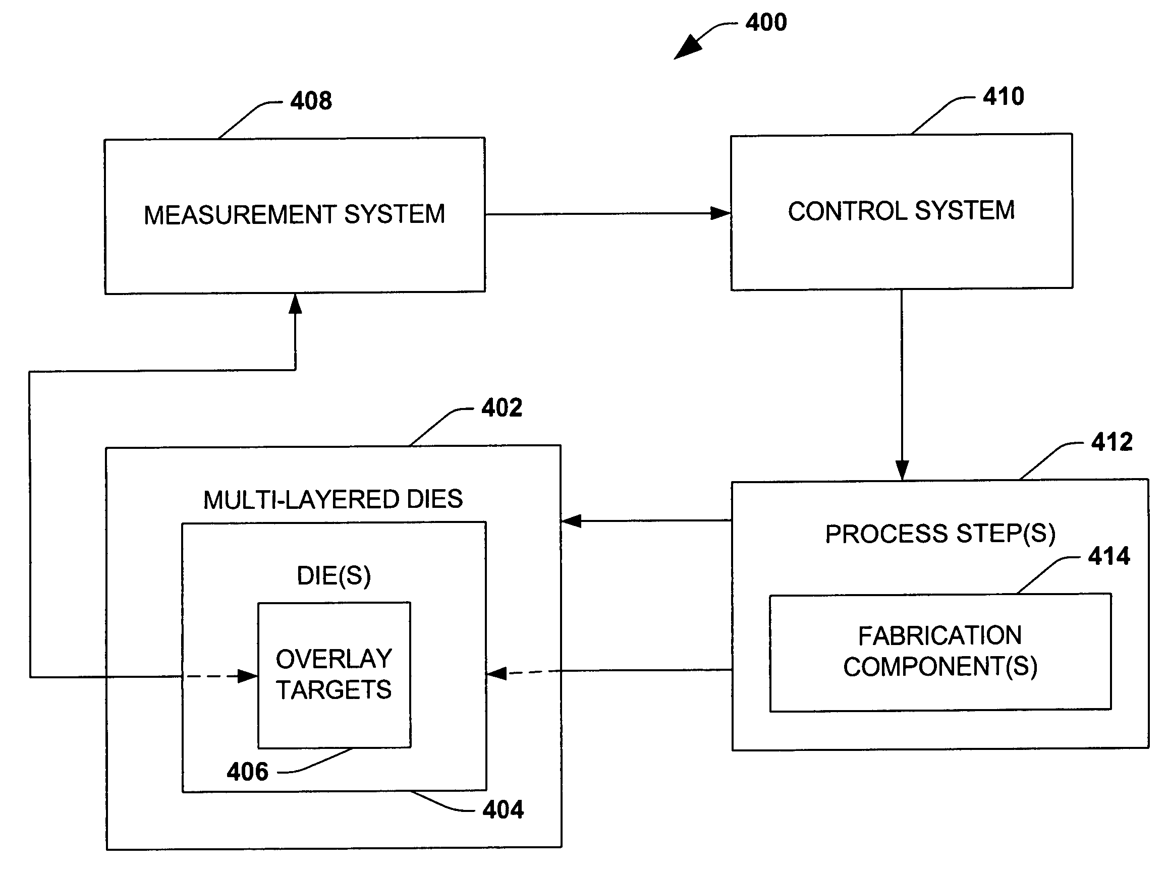
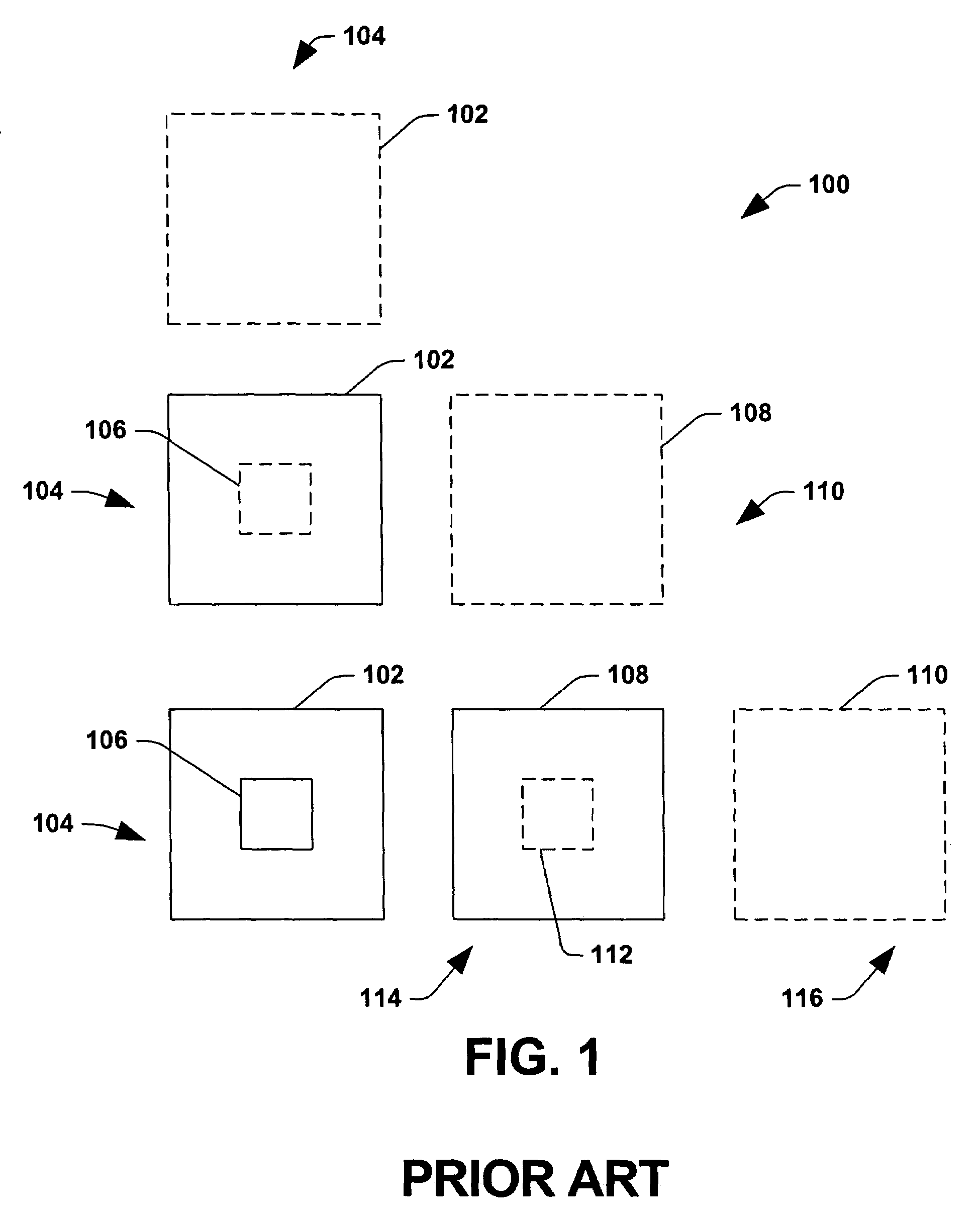
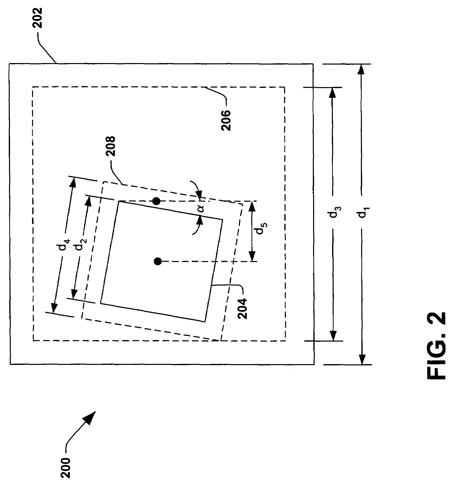
[0030]The present invention is now described with reference to the drawings, wherein like reference numerals are used to refer to like elements throughout. In the following description, for purposes of explanation, numerous specific details are set forth in order to provide a thorough understanding of the present invention. It may be evident, however, that the present invention may be practiced without these specific details. In other instances, well-known structures and devices are shown in block diagram form in order to facilitate describing the present invention.

[0031]As used in this application, the term “computer component” is intended to refer to a computer-related entity, either hardware, a combination of hardware and software, software, or software in execution. For example, a computer component may be, but is not limited to being, a process running on a processor, a processor, an object, an executable, a thread of execution, a program, and / or a computer. By way of illustrat...


PUM

PropertyMeasurementUnit
wavelengthsaaaaaaaaaa
dimensionaaaaaaaaaa
temperatureaaaaaaaaaa

Abstract

A system facilitating measurement and correction of overlay between multiple layers of a wafer is disclosed. The system comprises an overlay target that represents overlay between three or more layers of a wafer and a measurement component that determines overlay error existent in the overlay target, thereby determining overlay error between the three or more layers of the wafer. A control component can be provided to correct overlay error between adjacent and non-adjacent layers, wherein the correction is based at least in part on measurements obtained by the measurement component.

Description

TECHNICAL FIELD[0001]The present invention relates generally to monitoring and correcting a semiconductor manufacturing process. More particularly, the invention relates to a system and / or methodology for measuring and correcting overlay of multiple layers on an integrated circuit.BACKGROUND OF THE INVENTION[0002]In the semiconductor industry, there is a continuing trend toward higher device densities. To achieve these high densities, there has been and continues to be efforts toward scaling down device dimensions (e.g., at submicron levels) on semiconductor wafers. In order to accomplish such high device packing density, smaller and smaller feature sizes are required in integrated circuits (ICs) fabricated on small rectangular portions of the wafer, commonly known as dies. This can include width and spacing of interconnecting lines, spacing and diameter of contact holes, surface geometry such as corners and edges of various features as well as surface geometry of other features. To...

Claims


Application Information

Patent Timeline
Patent Type & Authority Patents(United States)
IPC IPC(8): G06F17/50G03C5/00G03F9/00G01N21/956G03F7/20H01L21/66H01L23/544
CPCG01N21/95607G03F7/70633H01L22/34H01L2924/0002H01L2924/00H01L22/12
Inventor PHAN, KHOI A.RANGARAJAN, BHARATHSINGH, BHANWAR
Owner GLOBALFOUNDRIES INC
Why Eureka
Try Eureka