Energy spectrum measuring apparatus, electron energy loss spectrometer, electron microscope provided therewith, and electron energy loss spectrum measuring method

a technology of energy spectrum and measuring apparatus, which is applied in the direction of instruments, material analysis using wave/particle radiation, nuclear engineering, etc., can solve the problems of false results, degrading energy precision and and affecting the accuracy of electron energy loss spectrum

Inactive Publication Date: 2006-06-27
HITACHI HIGH-TECH CORP
View PDF6 Cites 16 Cited by
  • Summary
  • Abstract
  • Description
  • Claims
  • Application Information

AI Technical Summary

Benefits of technology

[0022]The present invention allows automatically adjusting the focus of a spectrum.

Problems solved by technology

There used to be a problem that a pixel position changes when a trajectory of the electron beam changes because of an effect of an external electromagnetic field, thereby degrading energy precision and accuracy of the electron energy loss spectrum.
The degradation of the energy precision and accuracy of the electron energy loss spectrum causes the following problems when the electron energy loss spectrum at a specific location or multiple locations is measured on a specimen as described above.
When the element from the material B is identified based on spectra at individual measured points, there is a problem that a false result is obtained.

Method used


Image

  • Energy spectrum measuring apparatus, electron energy loss spectrometer, electron microscope provided therewith, and electron energy loss spectrum measuring method
  • Energy spectrum measuring apparatus, electron energy loss spectrometer, electron microscope provided therewith, and electron energy loss spectrum measuring method
  • Energy spectrum measuring apparatus, electron energy loss spectrometer, electron microscope provided therewith, and electron energy loss spectrum measuring method

Examples


second embodiment

[0082]The following section describes the present invention. FIG. 4(a) shows a schematic of a specimen to be measured. The specimen has a structure of laminating a material A (constituting element: A), a material with an unknown constituting element (constituting element is assumed to be B), and material and material C (constituting element C), and a line analysis is applied to the individual materials in a sequence of the material A, the material B, and the material C as shown in FIG. 4 (a).

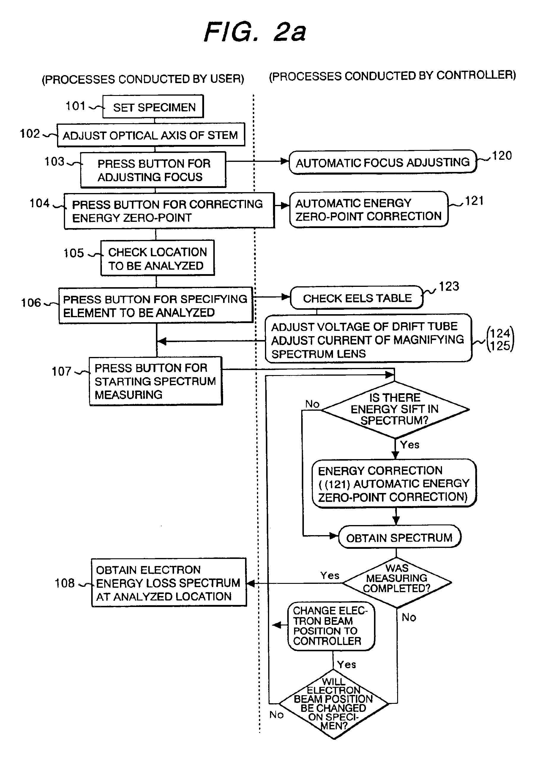
[0083]An operator simply (1) specifies a start point and an end point of a line to be measured, and (2) participates in a specification process for an element to be analyzed, or an energy range to be measured, and the controller 26 consecutively conducts the operations of (3) energy correction processing for the spectrum, (4) spectrum measuring, and (5) controlling the electron beam position on the specimen until the electron beam reaches the end point specified by the operator. An existence of ...

third embodiment

[0085]The following section describes the present invention. The energy can be corrected even when a zero-loss peak does not appear on the electron beam detector 13 with the apparatus of the present invention. (122) Automatic zero-loss electron retrieval in FIG. 2(e) shows the procedure of this process.

[0086]An operator simply presses the button to conduct the automatic zero-loss peak retrieval, for example, and the controller 26 (1) detects a position for the largest peak (zero-loss peak). If (1)′ the largest peak (zero-loss peak) does not exist on the electron beam detector 13, the drift tube 19 or the magnetic field sector 11 are controlled such that the zero-loss peak appears on the electron beam detector 13, (2) a deviation between the reference pixel position of the electron beam detector 13 and the zero-loss peak position appearing as the result of the operation (1) or (1)′, and (3) the drift tube 19 or the magnetic sector 11 are controlled so as to correct the deviation base...


PUM


Abstract

An electron beam detector detects a peak of a spectrum, and when a peak position is deviated from a reference position on the electron beam detector, a controller for controlling an electron beam position on the electron beam detector is used to correct a deviation. An electron energy loss spectrum is measured while controlling correction a deviation between an electron beam position on a specimen, and a peak position of the spectrum, and a spectrum measuring with the electron beam detector.

Description

[0001]The present application is a continuation of application Ser. No. 09 / 988,339, filed Nov. 19, 2001, now U.S. Pat. No. 6,703,613 the entire disclosure of which is incorporated herein by reference.BACKGROUND OF THE INVENTION[0002]The present invention relates to an electron energy loss spectrum measuring apparatus, a transmission electron microscope or a scanning transmission electron microscope, and an electron energy loss spectrum measuring method.[0003]As semiconductor devices and magnetic head elements become small and microscopic, the elements has a structure where thin films of several nm (nanometer) are laminated in an area of about submicron. Since the structure, the element distribution, the crystal structure, and the chemical bonding state of the micro area largely affect characteristics of the semiconductor elements and the magnetic head elements, it is important to analyze the micro area.[0004]Methods for observing the micro area include a scanning electron microscope...

Claims


Application Information

Patent Timeline
Patent Type & Authority Patents(United States)
IPC IPC(8): H01J47/00G01Q30/02G01Q30/06H01J37/252
CPCG01N23/2251H01J37/05H01J37/244H01J37/252H01J37/26H05H1/0037H01J37/28H01J2237/24485H01J2237/24495H01J2237/2487H01J2237/262H01J2237/2802
Inventor KAJL, KAZUTOSHIAOYAMA, TAKASHITAYA, SHUNROKUISAKOZAWA, SHIGETO
Owner HITACHI HIGH-TECH CORP
Why Eureka
Try Eureka