Control circuit and reconfigurable logic block

a logic block and control circuit technology, applied in the field of reconfigurable logic blocks, can solve the problems logic circuit reconfiguration, and achieve the effects of large-scale logic circuits and large-scale logic circuits

Active Publication Date: 2006-06-27
KK TOSHIBA
View PDF5 Cites 25 Cited by
  • Summary
  • Abstract
  • Description
  • Claims
  • Application Information

AI Technical Summary

Benefits of technology

[0010]The present invention was devised in response to the forgoing requirements, and aims to provide a reconfigurable logic block and a control circuit, so as to miniaturize a write or readout circuit for a memory array, miniaturize the entire circuit by providing a multi-level memory, and decrease logic circuit reconfiguration time.

Problems solved by technology

However, the reconfigurable logic block is large-scale since a memory array, which stores reconfiguration data for a to-be-rewritten logic circuit, is required.
Furthermore, when rewriting a logic circuit, it is necessary to serially transmit a large quantity of circuitry data from a memory to a circuit via a bus line.
Thus, a great deal of time is required for logic circuit reconfiguration.
In a current method, since writing and reading for the memory array is implemented, for example, in series in units of 16 bits, a great deal of time is required with a large-scale logic circuit.
Furthermore, even with rewriting logic circuit interconnects, reconfiguration is implemented in series, requiring a great deal of time.
Since each memory element must be provided with a write circuit and a sense amplifier, it is difficult to miniaturize the entire reconfigurable logic block.

Method used


Image

  • Control circuit and reconfigurable logic block
  • Control circuit and reconfigurable logic block
  • Control circuit and reconfigurable logic block

Examples


first embodiment

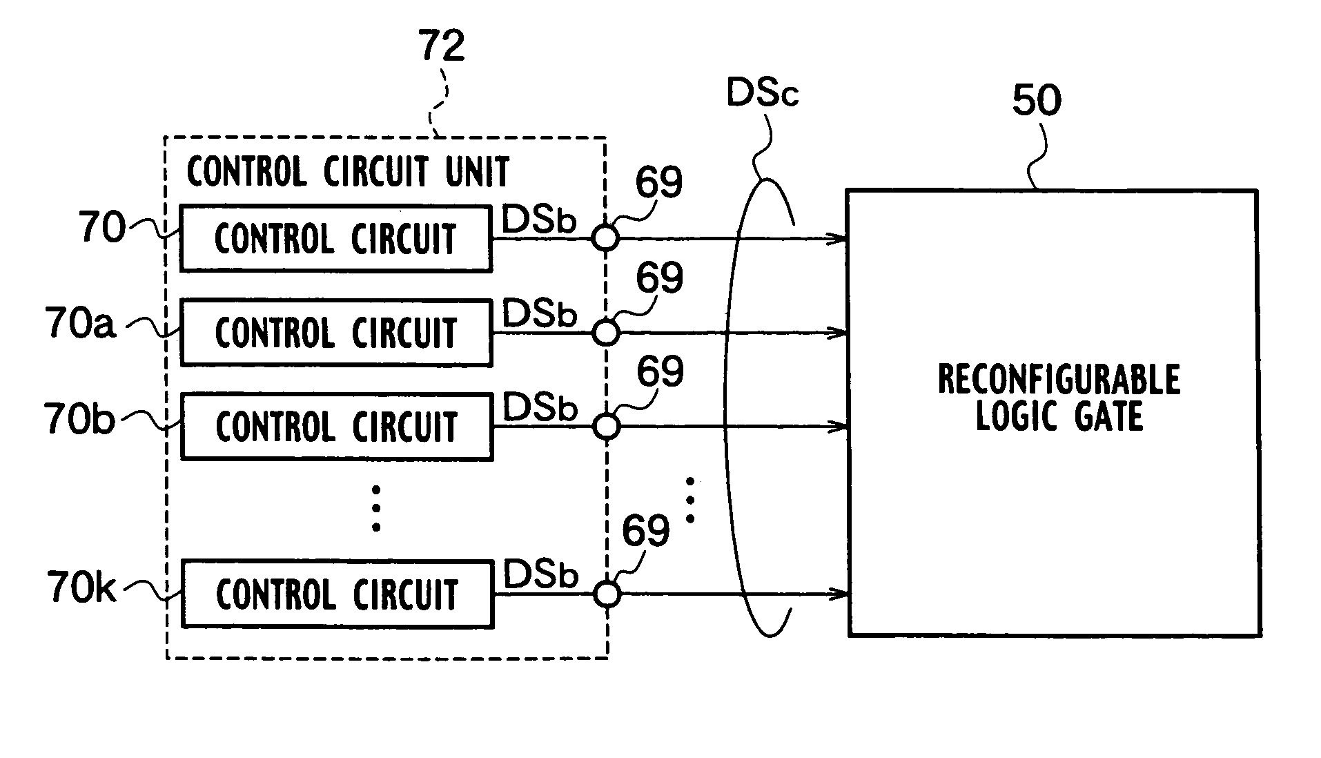
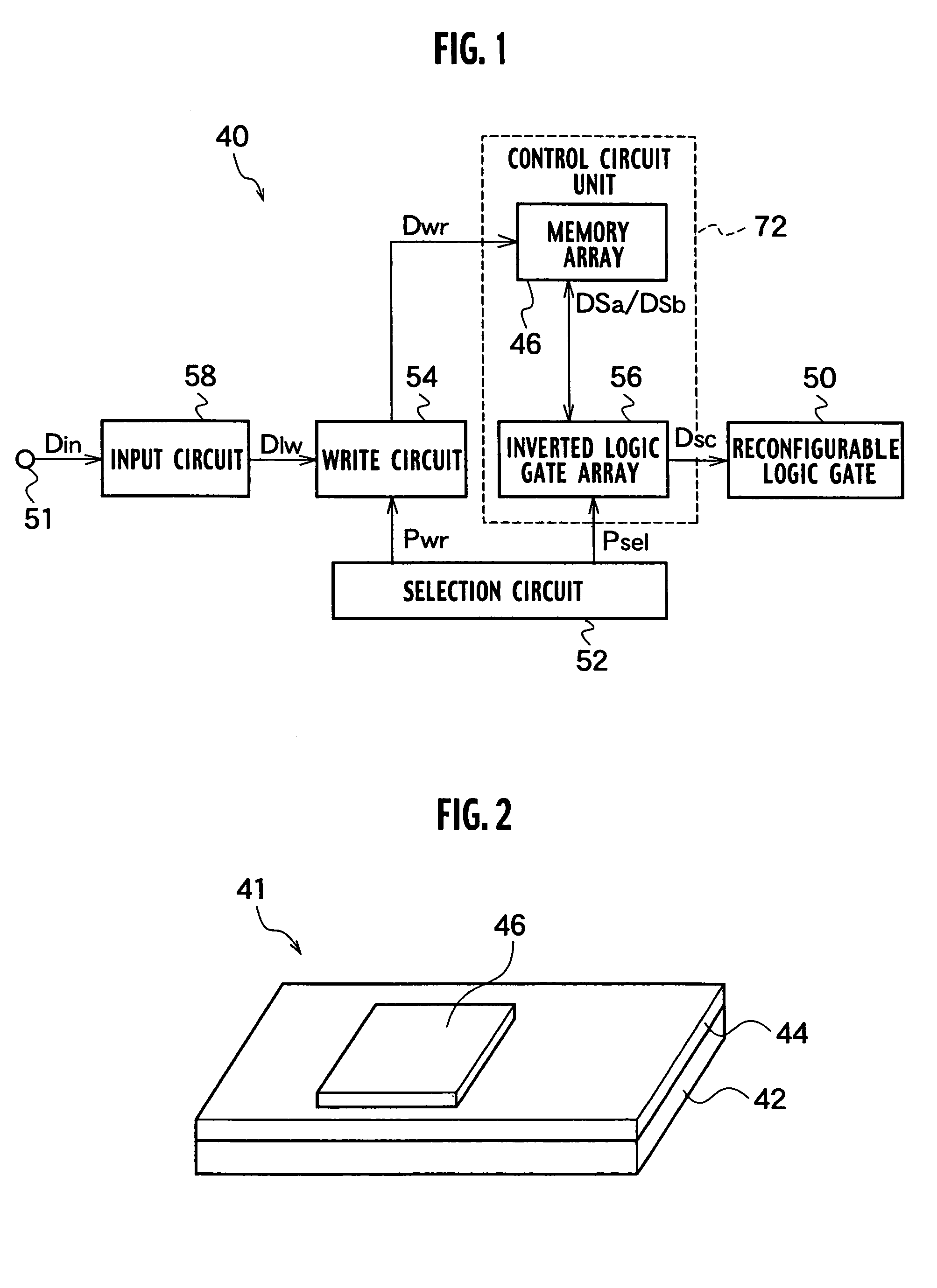
[0034]A reconfigurable logic block 40 according to a first embodiment of the present invention, as shown in FIG. 1, includes an input circuit 58 for acquiring an input signal Din including data used for implementing reconfiguration of logic gates for each of a plurality of logic circuits (hereinafter, referred to as ‘reconfiguration data’) from an input terminal 51 externally connected to, for example, a design system for a logic circuit layout (not shown in the drawing). A write circuit 54 is provided for transmitting a write signal Dwr corresponding to the reconfiguration data by amplifying and converting a circuitry data signal Dlw transmitted from the input circuit 58. A control circuit unit 72 has a memory array 46 storing the reconfiguration data for the plurality of logic circuits in accordance with the write signal Dwr and an inverted logic gate array 56 implementing logical operations based on the stored reconfiguration data by control signals DSa and DSb. The control circu...

second embodiment

[0050]A control circuit 170 of the reconfigurable logic block 40 according to a second embodiment of the present invention, as shown in FIG. 7, includes an inverted logic gate unit 68 providing a reset-set-latch (RS-latch) circuit, and a memory unit 64 inserted in the inverted logic gate unit 68. A first inverted logic gate 76a and a second inverted logic gate 76b in the inverted logic gate unit 68 include a set input terminal S and a reset input terminal R, respectively. A first variable resistive memory 64a is connected between the output terminal Ya of the first inverted logic gate 76a and an input terminal B of the second inverted logic gate 76b. A second variable resistive memory 64b is connected between an input terminal A of the first inverted logic gate 76a and an output terminal Yb of the second inverted logic gate 76b. Output terminals 69a and 69b of the control circuit 170 are connected to the first and second inverted logic gates 76a and 76b, respectively. NAND circuits ...

third embodiment

[0060]A reconfigurable logic block 40a according to a third embodiment of the present invention, as shown in FIG. 12, includes the input circuit 58 having an input terminal 51; a control circuit unit 72a having an inverted logic gate array 56a connected to the input circuit 58, and a memory array 46a connected to the inverted logic gate array 56a; a reconfigurable logic gate 50 connected to the inverted logic gate array 56a; and the selection circuit 52 connected to the inverted logic gate array 56a. The input circuit 58 acquires input signals Din including reconfiguration data of logic gates for a plurality of logic circuits from a design system for a logic circuit layout or the like, which is connected to the input terminal 51. The inverted logic gate array 56a, based on a write instruction signal Pwr from the select circuit 52, transmits a circuitry data signal Dlw from the input circuit 58a as a write signal Dwr to the memory array 46a so as to write in the reconfiguration data....


PUM


Abstract

A control circuit for providing a control signal to build a logic circuit includes a latch circuit including first and second inverted logic gates; a first variable resistive memory provided between an output of the first inverted logic gate and an input of the second inverted logic gate, the first variable resistive memory configured to store a resistance value in accordance with a write signal; and a resistive element provided between an input of the first inverted logic gate, wherein the output of the second inverted logic gate serves to transmit the control signal.

Description

CROSS REFERENCE TO RELATED APPLICATIONS[0001]This application is based upon and claims the benefit of priority from prior Japanese Patent Application P2003-335574 filed on Sep. 26, 2003; the entire contents of which are incorporated by reference herein.BACKGROUND OF THE INVENTION[0002]1. Field of the Invention[0003]The present invention relates to a reconfigurable logic block. More specifically, it relates to a control circuit for reading and writing circuitry data for a logic circuit in a memory element.[0004]2. Description of the Related Art[0005]A reconfigurable logic block rewrites a configuration of a logic circuit using software, and is effective as a means of providing an adaptable system large-scale integration (LSI). However, the reconfigurable logic block is large-scale since a memory array, which stores reconfiguration data for a to-be-rewritten logic circuit, is required. Furthermore, when rewriting a logic circuit, it is necessary to serially transmit a large quantity o...

Claims


Application Information

Patent Timeline
Patent Type & Authority Patents(United States)
IPC IPC(8): H03K19/173G06F7/38G11C8/00H03K19/177H03K19/20G11C11/412G11C7/00G11C7/10G11C13/00G11C16/02G11C16/10H01L21/82H01L27/10H01L27/105H03K3/037H03K3/45
CPCH03K3/45H03K19/1778H03K19/17748H03K19/1776H03K19/17728G11C16/02G11C16/10G11C5/06G11C7/10G11C13/0002G11C13/0021
Inventor FUJITA, SHINOBU
Owner KK TOSHIBA
Why Eureka
Try Eureka