Nano-antenna apparatus and method

a technology of nano-antennas and antennas, applied in the field of nano-antennas, can solve problems such as former energy radiating away, and achieve the effect of efficient uwb transmission

Inactive Publication Date: 2006-06-27
NEXT RF
View PDF3 Cites 14 Cited by
  • Summary
  • Abstract
  • Description
  • Claims
  • Application Information

AI Technical Summary

Problems solved by technology

Further, this volume may partition outside energy from inside energy, causing the former energy to radiate away.

Method used


Image

  • Nano-antenna apparatus and method
  • Nano-antenna apparatus and method
  • Nano-antenna apparatus and method

Examples


first alternate embodiment

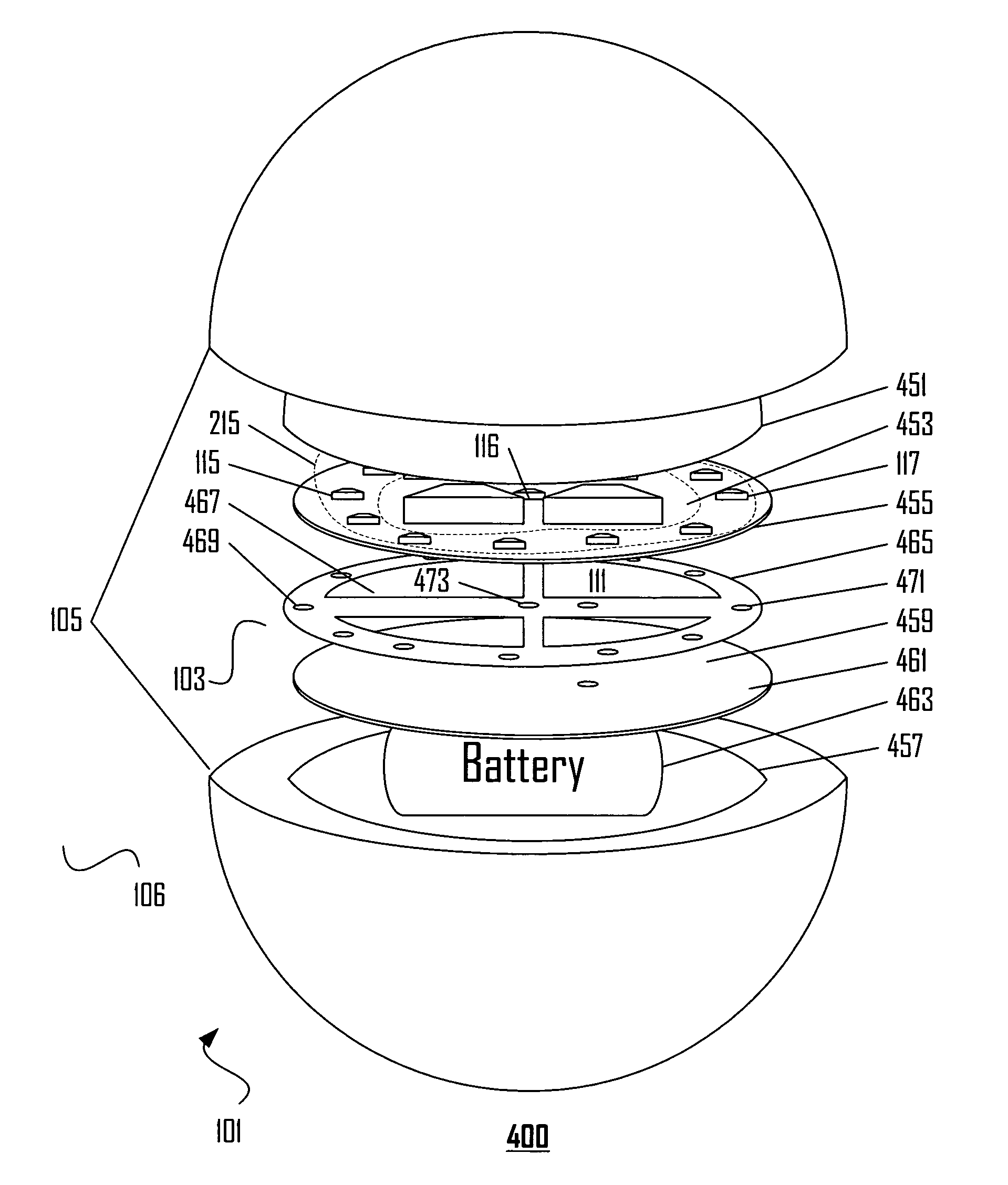
[0060]FIG. 5 is a schematic diagram 500 of a first alternate embodiment nano-antenna apparatus 501. First alternate embodiment nano-antenna apparatus 501 comprises a dielectric layer 505, a first conducting surface 507 and a second conducting surface 509. First conducting surface 507 and second conducting surface 509 are separated by a gap region 511. First alternate embodiment nano-antenna apparatus 501 occupies a volume that is substantially similar to a prolate spheroid.

[0061]Although in general an approximate symmetry in relative size is preferred, first conducting surface 507 is much smaller in extent than second conducting surface 509. In this embodiment, first conducting surface 507 is a protuberance on second conducting surface 509. Such an asymmetric form factor is preferred if the frequency content of a desired radiated signal is higher than would otherwise be radiated by a symmetric configuration. Shaping of first conducting surface 507 and second conducting surface 509 a...

second alternate embodiment

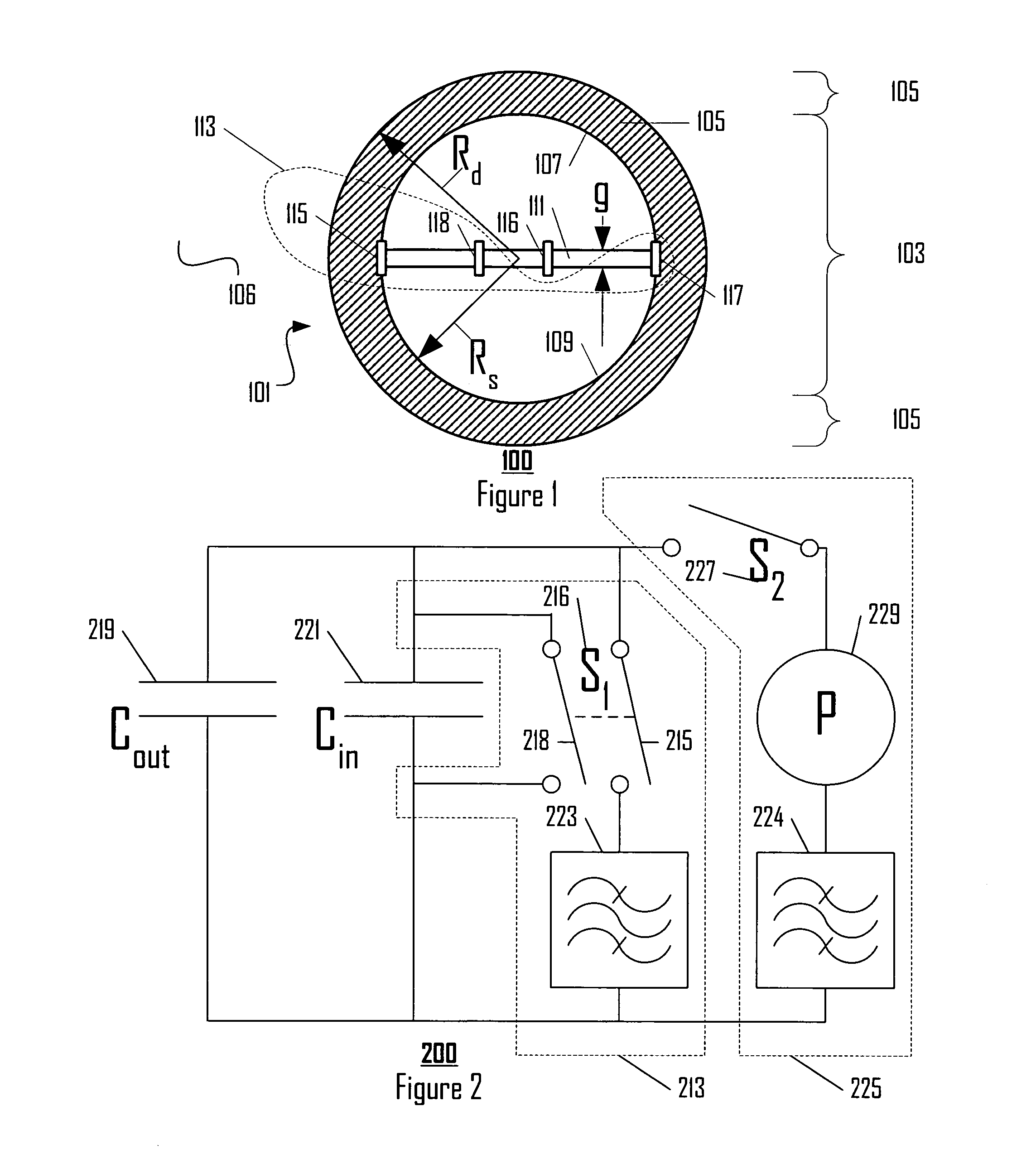
[0062]FIG. 6 is a schematic diagram 600 of a second alternate embodiment nano-antenna apparatus 601. Second alternate embodiment nano-antenna apparatus 601 comprises a dielectric layer 605, a first conducting surface 607 and a second conducting surface 609. First conducting surface 607 and second conducting surface 609 are separated by a gap region 611.

[0063]Second alternate embodiment nano-antenna apparatus 601 has an oblate spheroidal form factor. Such a form factor is useful where a predictable device orientation is preferred. For instance, if nano-antenna apparatus 601 were deployed out of an aerial vehicle, nano-antenna apparatus 601 would likely come to rest with short axis 675 in a substantially vertical orientation.

[0064]Further, gap region 611 has a serrated or meandering form factor. The extra length of this serrated or meandering form factor helps concentrate additional electrostatic energy outside nano-antenna apparatus 601, thus making nano-antenna apparatus 601 more ef...

third alternate embodiment

[0065]FIG. 7 is a schematic diagram 700 of a third alternate embodiment nano-antenna apparatus 701. Third alternate embodiment nano-antenna apparatus 701 comprises a dielectric layer 705, a first conducting surface 707 and a second conducting surface 709. A first conducting surface 707 and a second conducting surface 709 are separated by a gap region 711.

[0066]Third alternate embodiment nano-antenna apparatus 701 has an approximately Cartesian rectangular solid form factor, preferred for many consumer devices. Various ratios of height to width to depth may be appropriate for various applications. Third alternate embodiment nano-antenna apparatus 701 may also be more manufacturable.


PUM


Abstract

A nano-antenna apparatus (or equivalently a nano-antenna device) comprises a first conducting surface, a second conducting surface, a gap region between a first conducting surface and a second conducting surface and at least one discharge switch at least one discharge switch cooperates with first conducting surface, a second conducting surface to form a substantially continuous closed surface enclosing a volume. This volume may be substantially similar to a spheroid, a prolate spheroid, an oblate spheroid, a Cartesian rectangular solid or other shape. This volume may enclose at least one electric device. A dimension of the volume and a dielectric constant characterizing a dielectric layer may be chosen so as to yield a desired frequency response. Further, this volume may partition outside energy from inside energy, causing the former energy to radiate away.This invention further teaches a method for transmitting UWB impulse. This method comprises the steps of charging a first conducting surface with respect to a second conducting surface, and discharging a first conducting surface with respect to a second conducting surface such that the discharging forms a substantially continuous closed conducting shell from a first conducting surface and a second conducting surface. In alternate embodiments the discharging or charging may be adiabatic. Discharging may be positioned in time in accordance with a pulse position modulation scheme. Charging may be polarized in accordance to a flip or BPSK modulation scheme. Discharging may be effected by diodes, transistors, or MEMS devices.

Description

[0001]This application claims benefit of prior filed co-pending Provisional Patent Application Ser. No. 60 / 529,064 filed Dec. 12, 2003 which is incorporated herein by reference.BACKGROUND OF THE INVENTION[0002]1. Field of the Invention[0003]The present invention relates to antennas and more specifically to a system and method to utilize a conducting enclosure as a highly efficient electrically small antenna.[0004]2. Description of the Prior Art[0005]Ultra-wideband (UWB) systems are in great demand for precision tracking, radar, and communications. A commercially successful UWB system must be both small and very low power. Similarly, there is great interest at present in “smart dust,” miniature sensors, and other nano-devices that can wirelessly transmit data, positioning signals, or radar signals using very low power signals and utilizing wavelengths that may be much larger than the device itself. Highly efficient, electrically small antennas are a necessity for UWB systems, smart d...

Claims


Application Information

Patent Timeline
Patent Type & Authority Patents(United States)
IPC IPC(8): H01Q1/38H01Q1/26H01Q1/36H01Q5/00H01Q5/25H01Q9/00H01Q9/28
CPCH01Q1/36H01Q1/38H01Q5/25H01Q9/14H01Q9/28H01Q9/00
Inventor SCHANTZ, HANS GREGORY
Owner NEXT RF
Why Eureka
Try Eureka