BiCMOS electrostatic discharge power clamp

a technology of electrostatic discharge and power clamp, which is applied in the direction of semiconductors, electrical equipment, transistors, etc., can solve the problems of electronic products working abnormally, damage to parts and computer systems, and damage to major electronic parts or systems, so as to avoid leakage current problems, reduce the triggering voltage, and reduce the layout area

Inactive Publication Date: 2006-06-27
UNITED MICROELECTRONICS CORP
View PDF9 Cites 15 Cited by
  • Summary
  • Abstract
  • Description
  • Claims
  • Application Information

AI Technical Summary

Benefits of technology

[0012]Still another object is to utilize a BJT as a triggering element to trigger the MOS, and this can avoid the problems of leakage current and an undue layout area.
[0013]According to the objects mentioned above, the present invention discloses an ESD protecting circuit that combines a BJT with a MOS. The present invention utilizes the BJT as a triggering element. The base of the BJT is an open terminal and the MOS can be triggered by the connected method of the gate trigger, the base trigger, or the gate / base trigger. By utilizing the characteristics of the BJT, which can keep the current from leakage, and the problems associated with the prior art also can be avoided through a lower triggering voltage and a smaller layout area.
[0014]Therefore, the present invention utilizes a BJT as a triggering element to avoid the leakage current problem; moreover, the layout area is smaller than a RC triggering circuit and the triggering voltage also can be lower. Further, the ESD protecting circuit can sustain the heat resulted from ESD events while the ESD current flows through the substrate.

Problems solved by technology

An ESD event is the main reason resulting in the majority of electronic parts or systems damaged by an electrostatic overstress (EOS).
This kind of damage makes semiconductor parts and computer systems damaged forever, affecting the functionalities of integrated circuits (ICs), and causes electronic products work abnormally.
However, the damage caused from ESD is mostly produced by human beings, and is also difficult to avoid.
Without the desire, people provide a discharge path by contacting those objects to each other and damage the electronic parts or systems by an ESD event.
However, the technique of advanced process mentioned above and the smaller scaled parts can make the submicron CMOS ICs reduce the capability of ESD protection, and on the other hand, electrostatic produced by external environments is still the same as before.
Hence, the CMOS ICs damaged by ESD become more serious and many submicron CMOS ICs all face the same thorny problem.
However, the doped concentration has to be increased to achieve a zener diode with a lower breakdown voltage, and this can cause a leakage current problem.

Method used


Image

  • BiCMOS electrostatic discharge power clamp
  • BiCMOS electrostatic discharge power clamp
  • BiCMOS electrostatic discharge power clamp

Examples


Embodiment Construction

[0023]Some embodiments of the invention will now be described in greater detail. Nevertheless, it should be noted that the present invention can be practiced in a wide range of other embodiments besides those explicitly described, and the scope of the present invention is expressly not limited except as specified in the accompanying claims.

[0024]Further, it should be noted that the drawings are in greatly simplified form and they are not drawn to scale. Moreover, dimensions have been exaggerated in order to provide a clear illustration and understanding of the present invention.

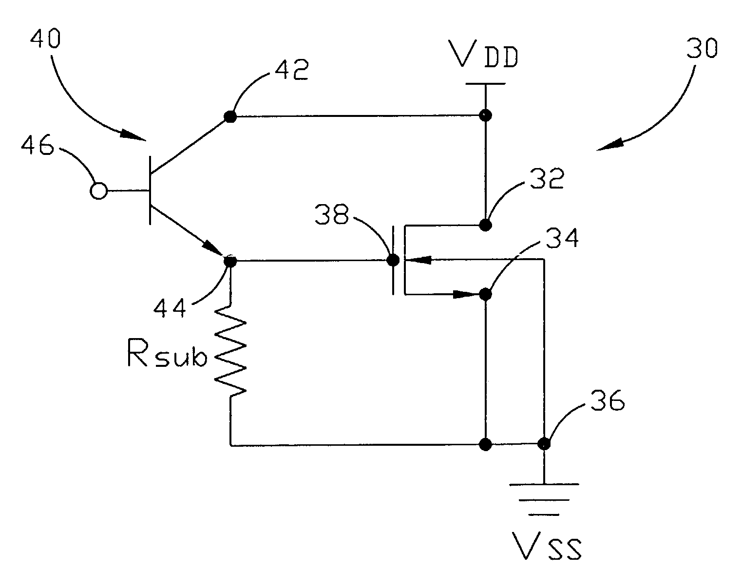
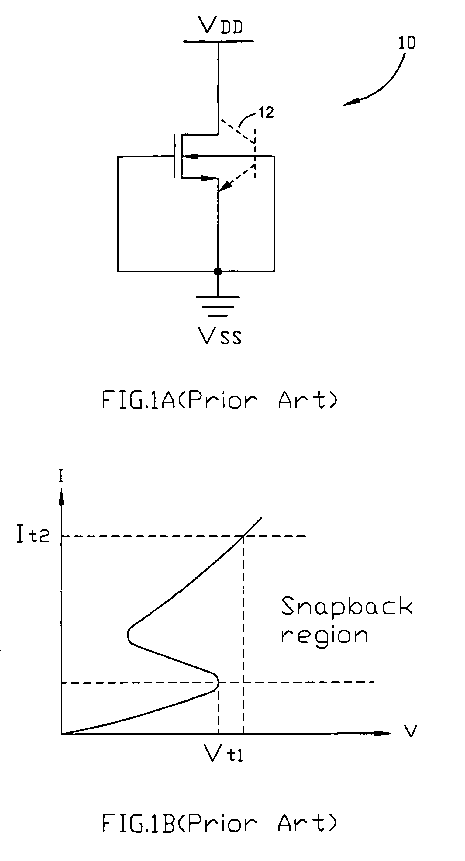
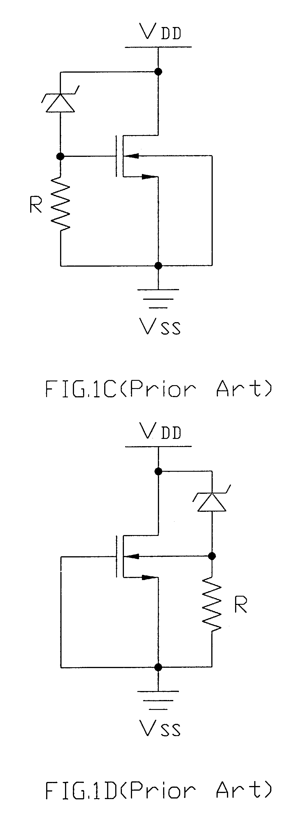
[0025]Referring to FIG. 2, an inner circuit 14 is among an input pad 12, an output pad 16, a positive voltage source VDD, and a ground VSS. Several ESD protecting circuits 21˜25 are placed between the positive voltage source VDD and the ground VSS to provide effective protection against any kinds of ESD models or paths.

[0026]As for using a MOS being an ESD path, the electrostatic current of the positive volta...


PUM


Abstract

A BiCMOS electrostatic discharge (ESD) protecting circuit is triggered by a bipolar junction transistor (BJT) for achieving ESD protection. Due to the layout area of the BJT ESD protecting circuit being smaller than the layout area of an RC circuit, layout area can be reduced. Moreover, the BJT reduces leakage current problems and has a lower triggering voltage. Therefore, the BJT in the ESD protecting circuit can effectively reduce problems of a higher triggering ESD voltage and leakage current.

Description

BACKGROUND OF THE INVENTION[0001]1. Field of the Invention[0002]This invention generally relates to the field of electrostatic discharge (ESD) protection of a metal oxide semiconductor (MOS). More particularly, the present invention relates to ESD protection of a BiCMOS.[0003]2. Description of the Prior Art[0004]An ESD event is the main reason resulting in the majority of electronic parts or systems damaged by an electrostatic overstress (EOS). This kind of damage makes semiconductor parts and computer systems damaged forever, affecting the functionalities of integrated circuits (ICs), and causes electronic products work abnormally. However, the damage caused from ESD is mostly produced by human beings, and is also difficult to avoid. Electrostatic energy can accumulate in human beings, apparatuses, storing devices, and even electronic parts or systems themselves during the processes of manufacture, assembly, testing, storage and shipping. Without the desire, people provide a discha...

Claims


Application Information

Patent Timeline
Patent Type & Authority Patents(United States)
IPC IPC(8): H02H9/00H01L27/02
CPCH01L27/0266
Inventor CHEN, SHIAO-SHIEN
Owner UNITED MICROELECTRONICS CORP
Why Eureka
Try Eureka