Model optimization for structures with additional materials

a technology of model optimization and structure, applied in the field of integrated circuit (ic) metrology, can solve problems such as wafer surface variations

Active Publication Date: 2006-07-04
TOKYO ELECTRON LTD
View PDF7 Cites 69 Cited by
  • Summary
  • Abstract
  • Description
  • Claims
  • Application Information

AI Technical Summary

Problems solved by technology

However, the steps under which a wafer is processed contain some deviations fr...

Method used


Image

  • Model optimization for structures with additional materials
  • Model optimization for structures with additional materials
  • Model optimization for structures with additional materials

Examples


Embodiment Construction

[0020]The following description is presented to enable one of ordinary skill in the art to make and use the invention and is provided in the context of a patent application and its requirements. In the following description, specific nomenclature is set forth to provide a thorough understanding of the present invention. It will be apparent to one skilled in the art that the specific details may not be necessary to practice the present invention. Furthermore, various modifications to the embodiments will be readily apparent to those skilled in the art and the generic principles herein may be applied to other embodiments. Thus, the present invention is not intended to be limited to the embodiments shown but is to be accorded the widest scope consistent with the principles and features described herein.

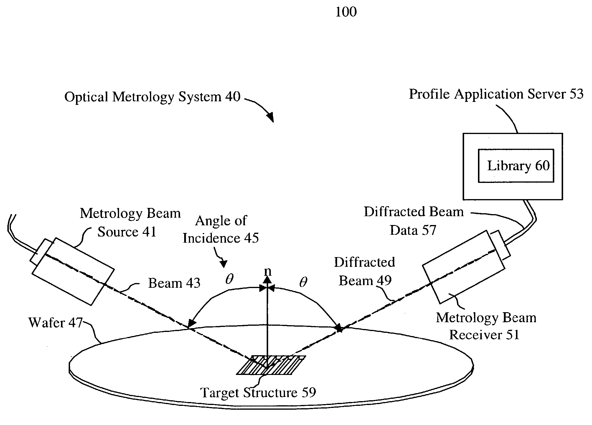
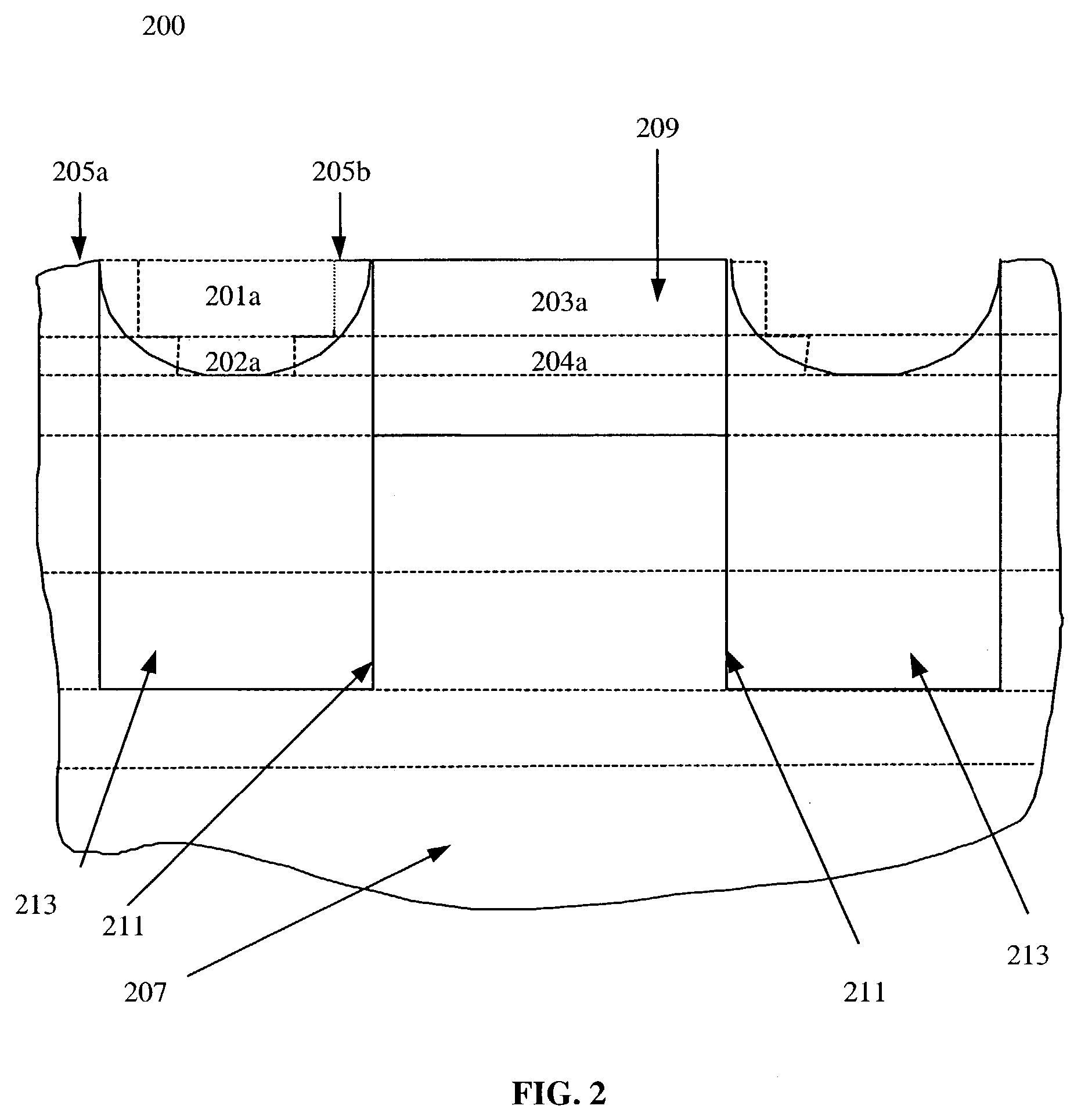
[0021]In order to facilitate the description of the present invention, an ellipsometric optical metrology system is used to illustrate the concepts and principles. It is understood that ...


PUM


Abstract

A wafer structure profile is modeled by determining one or more termination criteria. A determination is made as to whether a wafer structure includes at least one layer having three or more materials alone a line within the at least one layer. An optical metrology model for the wafer structure is created, where three or more materials are incorporated in the model for the at least one layer having three or more materials. A set of diffraction signals is simulated using the optical metrology model. The set of simulated diffraction signals and a set of diffraction signals measured off of the wafer structure are used to determine if the one or more termination criteria are met. The optical metrology model is modified until the one or more termination criteria are met.

Description

CROSS REFERENCE TO RELATED APPLICATIONS[0001]This application relates to co-pending U.S. patent application Ser. No. 09 / 727,530, entitled “System and Method for Real-Time Library Generation of Grating Profiles” by Jakatdar, et al., filed on Nov. 28, 2000; to co-pending U.S. patent application Ser. No. 10 / 206,491, entitled “Model and Parameter Selection in Optical Metrology” by Voung, et al., filed on Jul. 25, 2002; and to co-pending U.S. patent application Ser. No. 10 / 007,124, entitled “Optical Profilometry of Additional Material Deviations in a Periodic Grating”, by Niu, et al., filed on Dec. 4, 2001.BACKGROUND[0002]1. Field of the Invention[0003]The invention relates to integrated circuit (IC) metrology and more particularly to a method and system for optimizing wafer structure profile modeling.[0004]2. Related Art[0005]Growing demand for silicon wafers with large-scale integration necessitates submicron integrated circuit (IC) features with high precision and uniformity. As the f...

Claims


Application Information

Patent Timeline
IPC IPC(8): G01B11/24G01B11/06G01N21/47G01N21/95G01N21/956G03F7/20
CPCG01B11/0616G01N21/4788G01N21/9501G03F7/70616G03F7/70491G03F7/705G01N21/956G01N2021/95615G06F30/20
Inventor NIU, XINHUIJAKATDAR, NICKHIL
Owner TOKYO ELECTRON LTD
Why Eureka
Try Eureka