Flip-chip type semiconductor device and method of manufacturing the same

a semiconductor device and flip-chip technology, applied in semiconductor devices, semiconductor/solid-state device details, electrical devices, etc., can solve the problems of peeling phenomenon on the interface, limited application of the measure to a supercomputer, a large-scale computer, etc., and achieves high mounting reliability and low cost.

Inactive Publication Date: 2006-07-11
RENESAS ELECTRONICS CORP
View PDF6 Cites 14 Cited by
  • Summary
  • Abstract
  • Description
  • Claims
  • Application Information

AI Technical Summary

Benefits of technology

[0016]It is an object of the present invention to provide a flip-chip type semiconductor device which can be recycled, has high mounting reliability, and can be manufactured at a low cost and a method of manufacturing the same.
[0018]In the present invention, since the insulating resin layer is formed on the semiconductor substrate, even though a thermal stress or a mechanical stress acts on the metal bump, the stress acting on the metal bump can be moderated by the elasticity of the insulating resin layer. For this reason, an active region or the like formed on the semiconductor substrate can be more protected, and the mounting reliability of the semiconductor device is improved. In addition, since an under fill resin is not used unlike a conventional device, the semiconductor device can be recycled without damaging peripheral devices including the multi-layered wiring substrate. Furthermore, since the metal bump is formed on the electrode buried in the insulating resin layer to project from the surface of the support plate, the height between the semiconductor substrate and the metal bump can be increased. For this reason, when the semiconductor device is mounted on a multi-layered wiring printed board or the like, a standoff height which is the interval between the semiconductor substrate and the multi-layered wiring printed board can be increased. Therefore, when the semiconductor substrate and the multi-layered wiring printed board are offset due to the mismatch between the linear expansion coefficients of the semiconductor substrate and the multi-layered wiring printed board, the offset can be reduced. Especially the temperature cycle characteristics of the mounting reliability can be improved.
[0019]In the present invention, the periphery of the joint portion between the metal bump and the electrode is preferably covered with the insulating resin layer. In this manner, since the joint portion between the metal bump and the electrode is reinforced, the mechanical strength of the joint portion of the metal bump is improved to improve protection properties against an external stress.
[0020]Furthermore, in the present invention, for example, the support plate can be made of a conductive material, an insulating film and a metal film can be formed on the support plate in the order named, and a metal bump, having a ground potential, of the metal bumps can be connected to the metal film with a conductive adhesive agent. For example, the support plate can be made of an insulating material, a metal film can be formed on the surface of the support plate, and a metal bump, having a ground potential, of the metal bumps can be connected to the metal film with a conductive adhesive agent. In this manner, since the metal film can be used as a GND plane function, the following electric characteristics can be improved. That is, a GND inductance in a package form can be reduced, EMI (Electromagnetic wave impedance) shield effect can be improved, and crosstalk noise can be reduced.
[0024]In the present invention, since packages can be manufactured by the process in the state of a semiconductor device, the number of steps can be considerably reduced in comparison with a packaging method in which packages are manufactured from a conventional state of small pieces so that the cost can be considerably reduced.

Problems solved by technology

However, after the conventional flip-chip type semiconductor device 100 is mounted on the multi-layered wiring substrate 102, due to incoincidence (mismatch) between linear expansion coefficients of the multi-layered wiring substrate 102 and the flip-chip type semiconductor device 100, especially, the temperature cycle characteristics of the mounting reliability are degraded disadvantageously.
However, since the expensive ceramic-based material is used as the material of the multi-layered wiring substrate, the application of the measure is limited to a super computer, a large-scale computer, or the like which is generally maximally expensive.
However, in this conventional technique, when a void exists in the under fill resin, or when the adhesive characteristics of an interface between the under fill resin and the semiconductor chip and an interface between the under fill resin and the multi-layered wiring substrate using an organic material are poor, in a moist absorption reflow process of a product, a peeling phenomenon occurs on the interface, and a defective product is manufactured disadvantageously.
For this reason, the conventional technique cannot reliably advance a reduction in cost of a flip-flop type semiconductor device.
In addition, since a flip-chip type semiconductor chip is generally used in an LSI having high performance, the products itself is expensive.
However, when an under fill resin is interposed between the semiconductor chip and the multi-layered wiring substrate using an organic material, the semiconductor chip cannot be recycled.
In this case, since peripheral devices including the multi-layered wiring substrate using the organic material become defective, a reduction in cost can hardly be always advanced by using the multi-layered wiring substrate using the organic material.
For this reason, the non-defective semiconductor chip may be defective.
In this manner, due to the above-described problem, it is difficult to recycle a non-defective flip-chip type semiconductor chip in the conventional technique.

Method used


Image

  • Flip-chip type semiconductor device and method of manufacturing the same
  • Flip-chip type semiconductor device and method of manufacturing the same
  • Flip-chip type semiconductor device and method of manufacturing the same

Examples


first embodiment

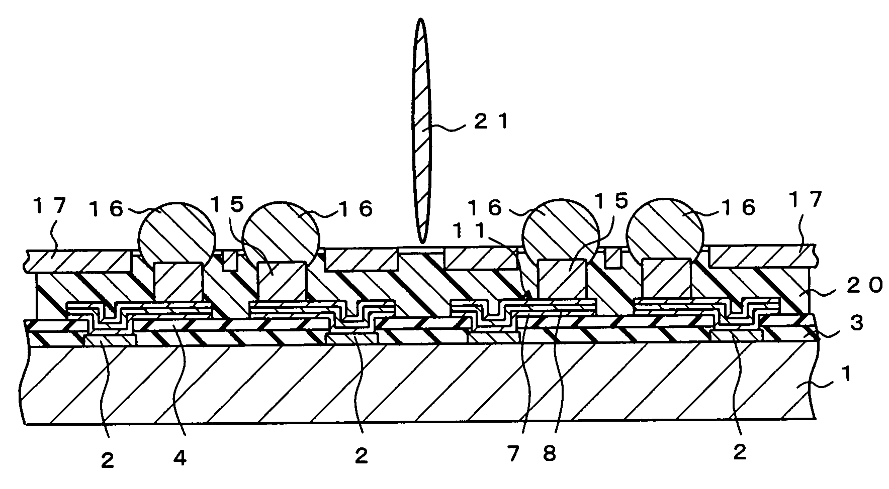
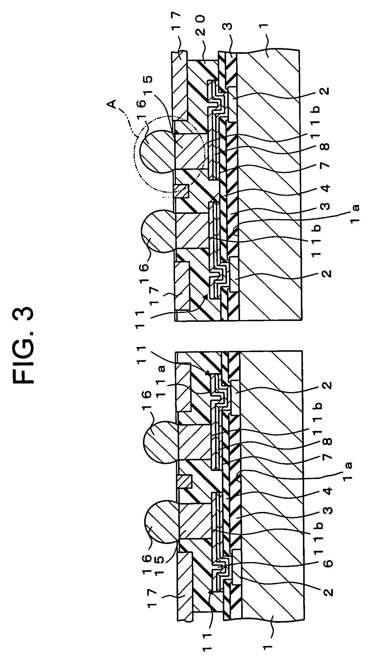
[0045]A flip-chip type semiconductor device according to an embodiment of the present invention and a method of manufacturing the same will be described below with reference to the accompanying drawings. FIG. 3 is a sectional view showing a flip-chip type semiconductor device according to the present invention, and FIG. 4 is an enlarged view of a section shown by two-dot chain line A in FIG. 3. In the flip-chip type semiconductor device of this embodiment, pad electrodes 2 are formed on the semiconductor substrate 1 as external terminal electrodes such that the pad electrodes 2 are located on the peripheries of chips in units of chips. The portion of the semiconductor substrate 1 that is between the pad electrodes 2 serves as an active region 1a. A passivation film 3 is formed on the active region 1a and an outer edge portion of the semiconductor substrate 1. An insulating resin layer 4 for protecting a re-wiring layer is formed on the passivation film 3. An opening 6 is formed abov...

second embodiment

[0079]A method of manufacturing a flip-chip type semiconductor device according to this embodiment will be described below. FIGS. 16A and 16B are sectional views sequentially showing steps in manufacturing a flip-chip type semiconductor device according to the present invention, and FIGS. 17A and 17B are sectional views sequentially showing the steps next to the steps in FIGS. 16A and 16B.

[0080]In this embodiment, the same steps as the steps up to the step shown in FIG. 12A in the manufacturing method of the first embodiment are used. An explanation will be started from the step next to the step shown in FIG. 12A.

[0081]As shown in FIG. 16A, height adjustment jigs 19 each having a predetermined height are arranged on both the sides of the semiconductor substrate 1, and the support plate 17a in which holes having diameters larger than that of the solder bumps 16a, 16b, and 16c are formed in the same pattern as the arrangement pattern of the solder bumps 16a, 16b, and 16c is arranged o...


PUM


Abstract

In a flip-chip type semiconductor device, a pad electrode and a passivation film are formed on a semiconductor substrate. An insulating resin layer is formed on the passivation film, and an opening is formed above the electrode. A pad electrode adhesive metal film is formed on the substrate like a re-wiring pattern, and a plating feed layer metal film and a Cu plating layer are sequentially formed on the metal film to form a wiring layer. A metal post electrode is formed on the wiring layer. A solder bump is formed on the post electrodes, a support plate in which holes each having a diameter larger than the diameter of the solder bump are formed at positions adjusted to the solder bumps is arranged, and an insulating resin layer is formed between the support plate and the semiconductor substrate. Therefore, a stress acting on the solder bump is moderated.

Description

CROSS-REFERENCE TO RELATED APPLICATION[0001]This application is a Divisional Application of application ser. No. 09 / 789,864, filed on Feb. 21, 2001, now U.S. Pat. No. 6,734,566 which claimed foreign priority of Japan application No. 2000-043665 file Feb. 21, 2000.BACKGROUND OF THE INVENTION[0002]1. Field of the Invention[0003]The present invention relates to a flip-chip type semiconductor device obtained by mounting a semiconductor chip on a multi-layered wiring substrate and a manufacturing method of the same and, more particularly, to a flip-chip type semiconductor device which can be recycled, has high mounting reliability, and can be manufactured at a low cost and a method of manufacturing the same.[0004]2. Description of the Related Art[0005]FIG. 1A is an illustration showing a conventional flip-chip type semiconductor device, and FIG. 1B is an illustration showing a mounting state of a conventional flip-chip type semiconductor device.[0006]As shown in FIG. 1A, in a conventiona...

Claims


Application Information

Patent Timeline
Patent Type & Authority Patents(United States)
IPC IPC(8): H01L21/44H01L23/12H01L21/56H01L21/60H01L23/485
CPCH01L24/13H01L24/11H01L2224/1147H01L2224/1191H01L2924/014H01L2224/13022H01L2224/13099H01L2224/16225H01L2224/75252H01L2924/01004H01L2924/01005H01L2924/01013H01L2924/01022H01L2924/01029H01L2924/01033H01L2924/01057H01L2924/01075H01L2924/01077H01L2924/01078H01L2924/01079H01L2924/09701H01L2924/30107H01L2924/3011H01L2924/3025H01L2924/01006H01L2924/01024H01L2924/01047H01L2924/00H01L24/03H01L24/05H01L2224/02377H01L2224/05001H01L2224/05008H01L2224/05022H01L2224/05024H01L2224/05569H01L2224/11H01L2224/13H01L2224/13025H01L2924/351H01L21/60
Inventor HONDA, HIROKAZU
Owner RENESAS ELECTRONICS CORP
Why Eureka
Try Eureka