Self-aligned trench MOSFETs and methods for making the same

Inactive Publication Date: 2006-07-18
SEMICON COMPONENTS IND LLC
View PDF371 Cites 72 Cited by
  • Summary
  • Abstract
  • Description
  • Claims
  • Application Information

AI Technical Summary

Benefits of technology

[0010]The present invention provides self-aligned trench MOSFETs and methods for manufacturing the same. By having a self-aligned structure, the number of MOSFETS per unit area—the cell density—is increased, increasing performance and making the MOSFETs cheaper to produce. The self-aligned structure for the MOSFET is provided by making the sidew

Problems solved by technology

Otherwise, power is wasted and excessive heat may be generated.
One problem standing in the way of inc

Method used


Image

  • Self-aligned trench MOSFETs and methods for making the same
  • Self-aligned trench MOSFETs and methods for making the same
  • Self-aligned trench MOSFETs and methods for making the same

Examples


Example

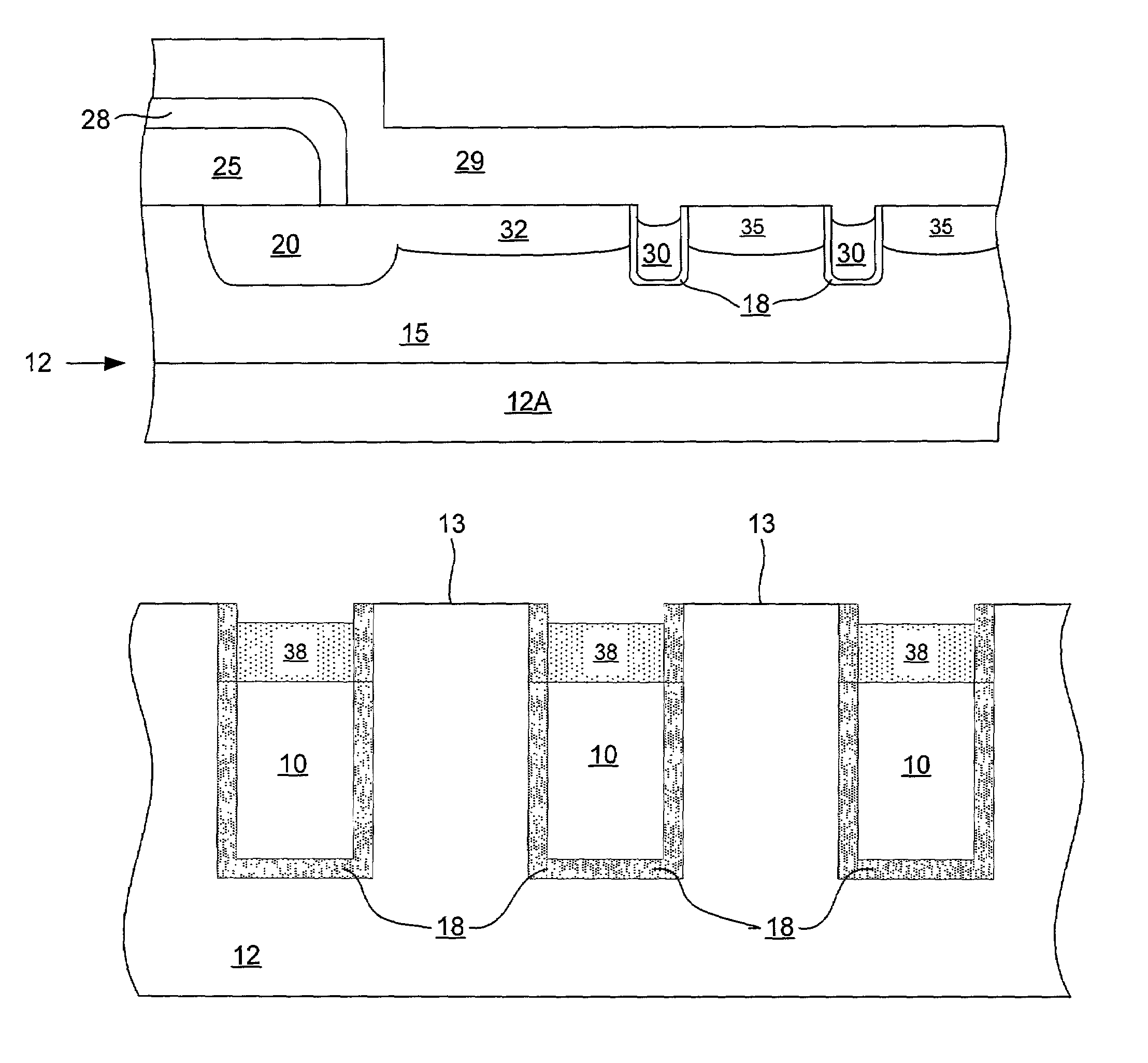
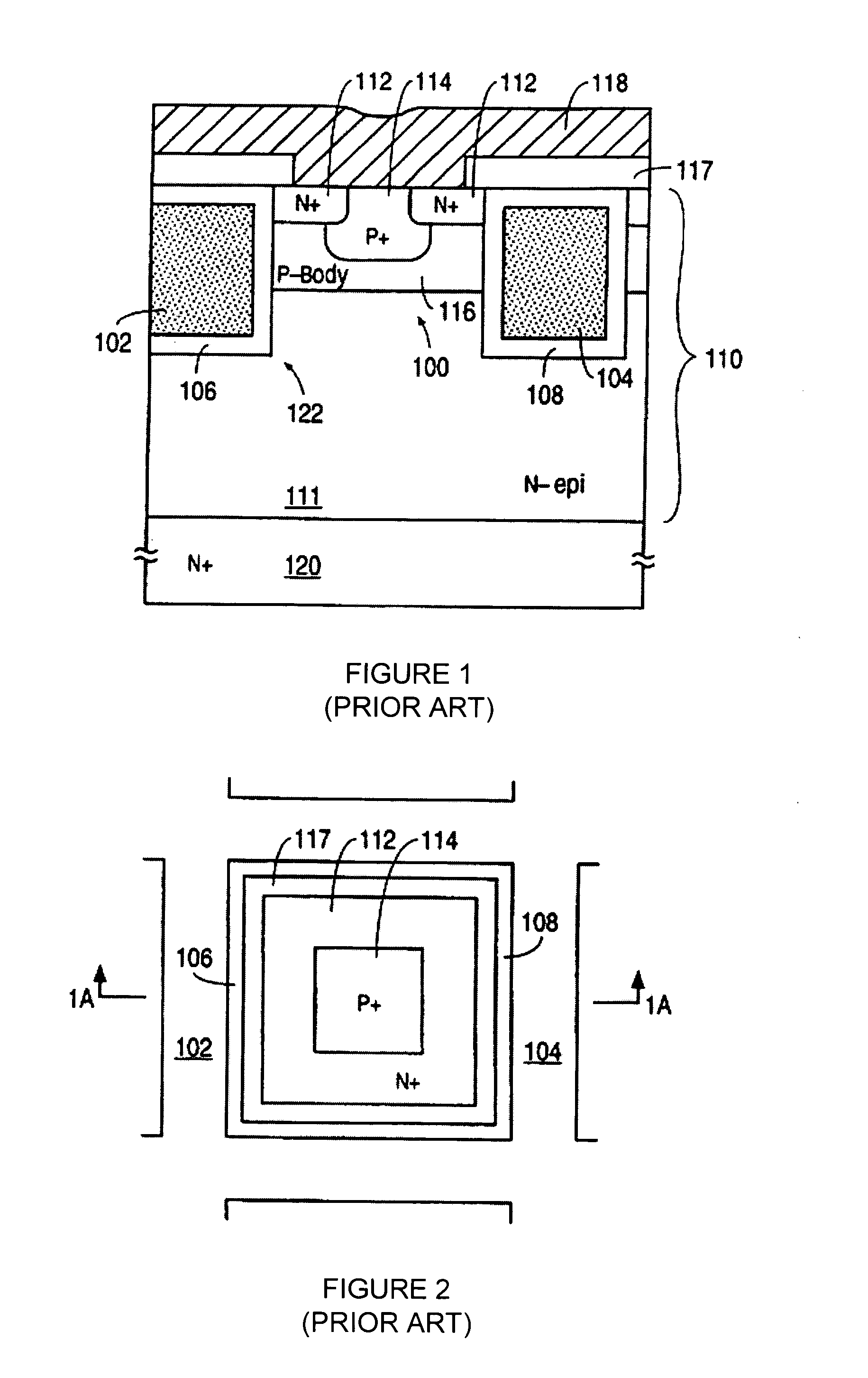
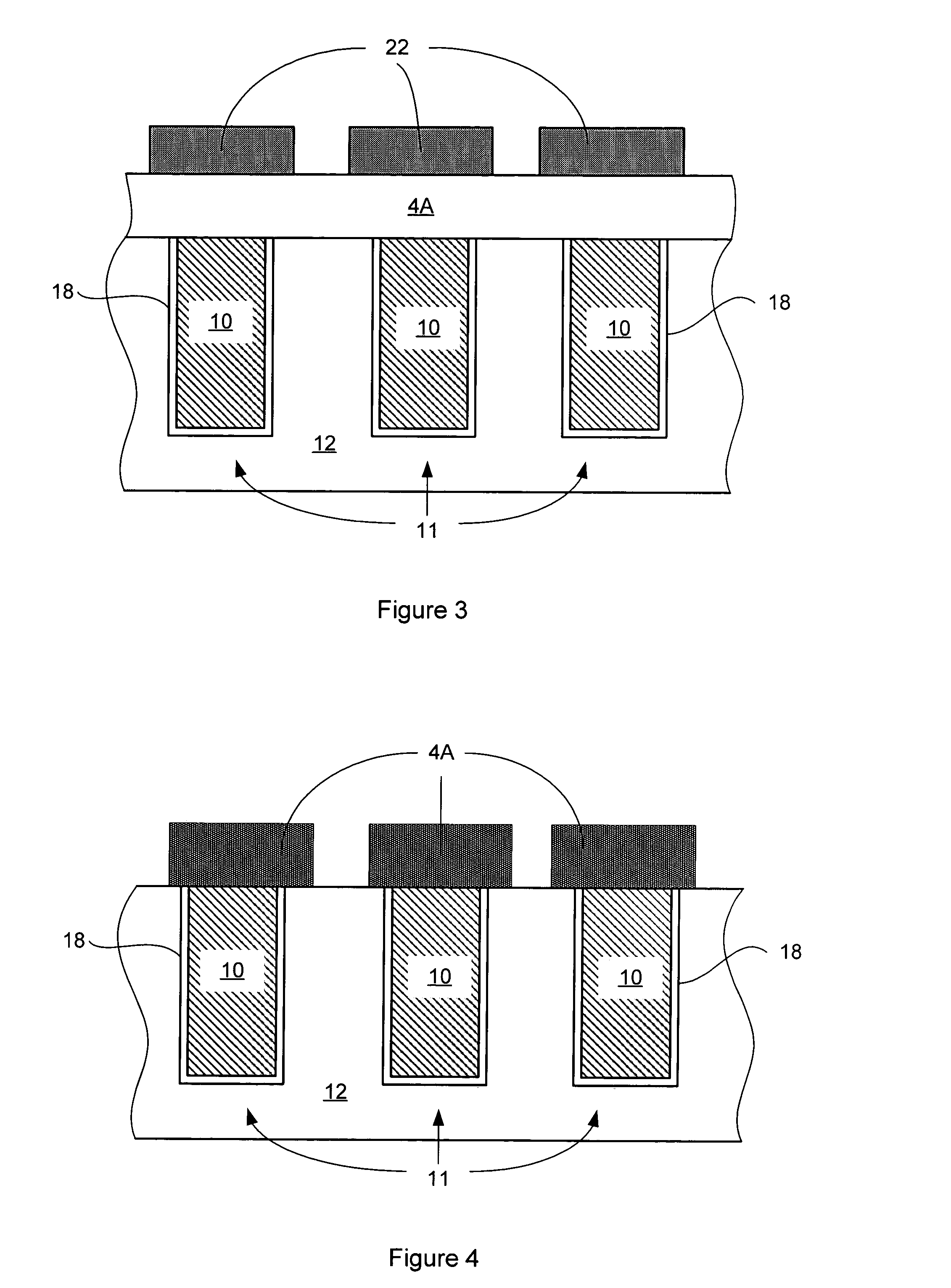
[0020]The following description provides specific details in order to provide a thorough understanding of the present invention. The skilled artisan, however, would understand that the present invention can be practiced without employing these specific details. Indeed, the present invention can be practiced by modifying the illustrated structure and method, and can be used in conjunction with apparatus and techniques conventionally used in the industry. For example, while the invention is described with reference to MOSFET devices, it could be modified for other devices formed in trenches which need to be isolated, such as bipolar devices, BDCMOS devices, or other types of transistor structures. As well, although the devices of the invention are described with reference to a particular type of conductivity (P or N), the devices can be configured with the opposite type of conductivity (N or P, respectively) by appropriate modifications.

[0021]FIGS. 5–14 illustrate one aspect of the pr...


PUM


Abstract

Self-aligned trench MOSFETs and methods for manufacturing the same are disclosed. By having a self-aligned structure, the number of MOSFETS per unit area—the cell density—is increased, making the MOSFETs cheaper to produce. The self-aligned structure for the MOSFET is provided by making the sidewall of the overlying isolation dielectric layer substantially aligned with the sidewall of the gate conductor. Such an alignment can be made through any number of methods such as using a dual dielectric process, using a selective dielectric oxidation process, using a selective dielectric deposition process, or a spin-on-glass dielectric process.

Description

FIELD OF THE INVENTION[0001]The invention generally relates to methods for fabricating integrated circuits (ICs) and semiconductor devices and the resulting structures. More particularly, the invention relates to metal oxide semiconductor field effect transistor (MOSFET) devices and methods for making such devices. Even more particularly, the invention relates to self-aligned trench MOSFET devices and methods for making such devices.BACKGROUND OF THE INVENTION[0002]There are numerous devices comprising silicon layers containing deep or high aspect ratio trenches. Forming such deep trenches in the silicon layer of these devices provides many novel and promising structures. The types of devices containing such trenches include the numerous types of silicon-based MEMS devices, as well ICs.[0003]In IC fabrication, devices such as transistors may be formed on a semiconductor wafer or substrate, which is typically made of silicon. MOSFET devices are widely used in numerous applications, i...

Claims


Application Information

Patent Timeline
IPC IPC(8): H01L21/8232H01L21/336H01L21/8234H01L27/088
CPCH01L27/088H01L21/823487
Inventor CHAU, DUCLOSEE, BECKYMARCHANT, BRUCEPROBST, DEANHERRICK, ROBERTMURPHY, JAMES
Owner SEMICON COMPONENTS IND LLC
Why Eureka
Try Eureka