Method and system for producing semiconductor devices

a technology of semiconductor devices and manufacturing methods, applied in the field of methods and systems for producing semiconductor devices, can solve the problems of inability to achieve high throughput, inability to reduce manufacturing costs, and inability to reduce throughpu

Inactive Publication Date: 2006-07-18
KK TOSHIBA
View PDF18 Cites 5 Cited by
  • Summary
  • Abstract
  • Description
  • Claims
  • Application Information

AI Technical Summary

Problems solved by technology

However, a very large number of shots of the electron beam are required and thus a reduction in throughput is inevitable.
If the VSB method increases in use, the effect of reducing the number of shots, which is created by adopting the CP method, is lessened naturally; therefore, a high throughput cannot be achieved.
Since a CP aperture is required for each product, manufacturing costs cannot be decreased, nor can be time periods.
1) The number of shots of electron beam is the smallest or the throughput of exposure is the highest.
2) Electron beam exposure is performed using a previously formed CP aperture.
3) The chip area of a device to be manufactured is the smallest.
4) The power consumption of a device to be manufactured is the lowest.
5) The operating frequency of a device to be manufactured is the highest.
However, the designer cannot take into consideration all the contents that are subject to constraints in terms of a process.
Consequently, the designer and engineer are satisfied with the parameters for the process and design, but they have no other choice but to take a very inefficient exposure method for the other parameters.
This leads to the design and exposure method that do not necessarily meet the user's needs in manufacturing a semiconductor device.
The above process therefore has the problem that the manufacturing costs and periods cannot meet the needs of a user.

Method used


Image

  • Method and system for producing semiconductor devices
  • Method and system for producing semiconductor devices
  • Method and system for producing semiconductor devices

Examples


first embodiment

(First Embodiment)

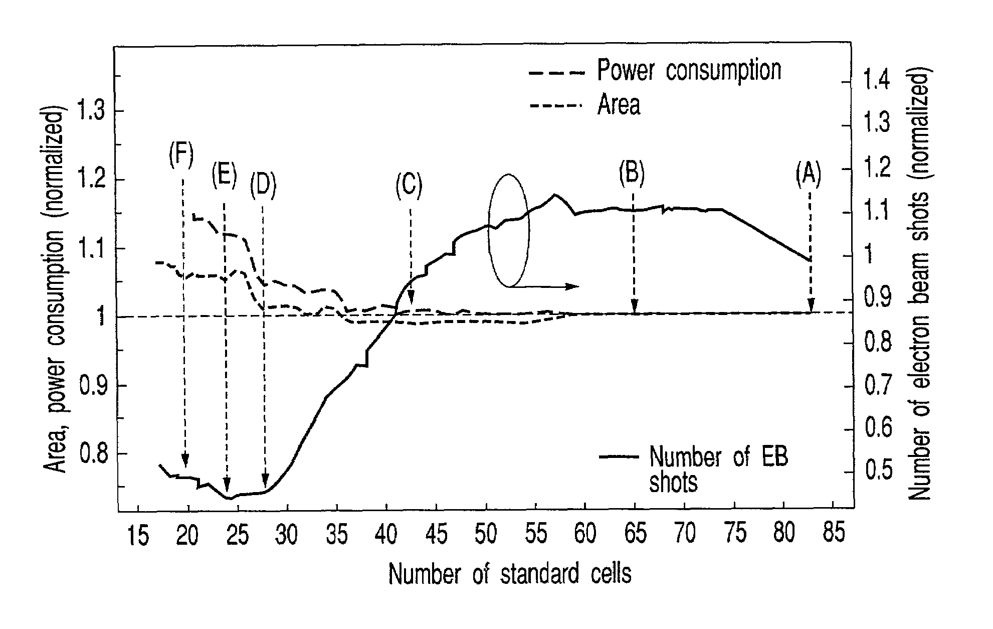
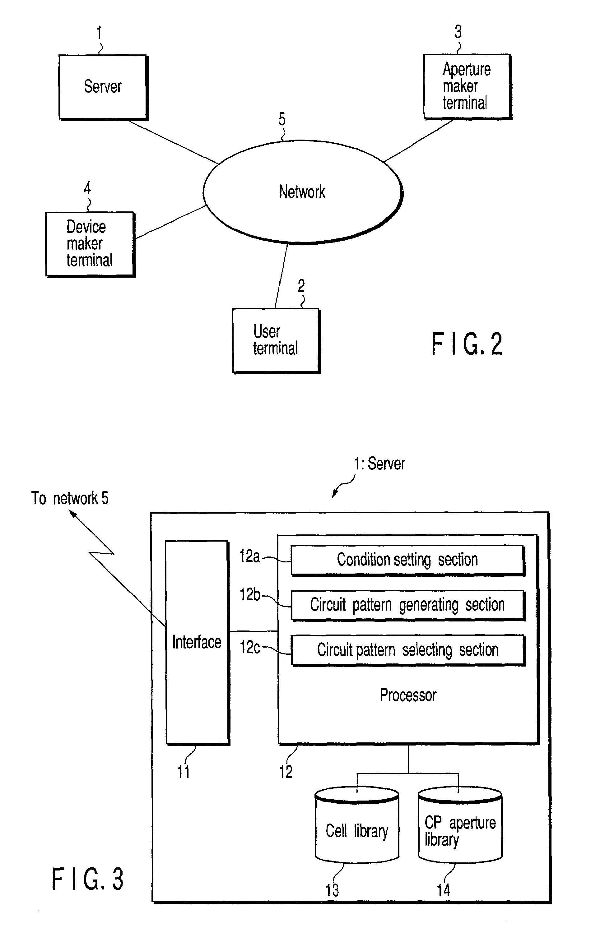
[0043]FIG. 2 shows a network structure of a semiconductor-device production system according to a first embodiment of the present invention. This production system includes a server 1, a user terminal 2, an aperture maker terminal 3, a device maker terminal 4, and a network 5.

[0044]The server 1 is a server operated by a system operator for operating the production system as a person who wishes to receive an order. The user terminal 2 is a terminal used by a plurality of users for using the production system as a person who wishes to place an order. The aperture maker terminal 3 is a terminal used by an aperture maker who produces apertures based on an order by the server 1. The device maker terminal 4 is a terminal used by a device maker who produces devices based on an order by the server 1. The server 1, user terminal 2, aperture maker terminal 3, and device maker terminal 4 are connected to the network 5. This connection can be established by wire or radio. Furt...


PUM

PropertyMeasurementUnit
operating frequencyaaaaaaaaaa
frequencyaaaaaaaaaa

Abstract

A user is requested to input specifications of a semiconductor device. Based on the specifications, a plurality of circuit patterns are generated by a CP method, and a design parameter is calculated for each of the circuit patterns. The user is provided with information of the plurality of circuit patterns together with the design parameters. The user selects a desired circuit pattern, whereas the server calculates manufacturing costs of the device and presents them to the user. The user checks the costs and then places an order.

Description

CROSS-REFERENCE TO RELATED APPLICATIONS[0001]This application is based upon and claims the benefit of priority from the prior Japanese Patent Application No. 2000-227324, filed Jul. 27, 2000, the entire contents of which are incorporated herein by reference.BACKGROUND OF THE INVENTION[0002]1. Field of the Invention[0003]The present invention relates to a method for producing a semiconductor device by charged-particle beam exposure using a character projection (CP) method and a system for producing the semiconductor device.[0004]2. Description of the Related Art[0005]Electron-beam exposure is an effective means for processing a fine pattern of a semiconductor circuit.[0006]In a variable shaped beam (VSB) method that is a typical electron-beam exposure method, a circuit pattern is divided into very small rectangles and triangles and these are repeatedly exposed to an electron beam. It is thus unnecessary to prepare a mask dedicated to the exposure of the pattern. However, a very large...

Claims


Application Information

Patent Timeline
Patent Type & Authority Patents(United States)
IPC IPC(8): G06G7/34G06F7/02G06F9/44G06F15/82G03F7/20G05B19/418G06Q50/00G06Q50/04H01J37/302H01L21/027
CPCG06Q20/20H01J37/3026H01J2237/31762Y02P90/02
Inventor INANAMI, RYOICHIMAGOSHI, SHUNKOOKUMURA, KATSUYA
Owner KK TOSHIBA
Why Eureka
Try Eureka