

Sacrificial oxide for minimizing box undercut in damascene FinFET
- Summary
- Abstract
- Description
- Claims
- Application Information
AI Technical Summary
Benefits of technology
Problems solved by technology
Method used
Image

Examples
Embodiment Construction
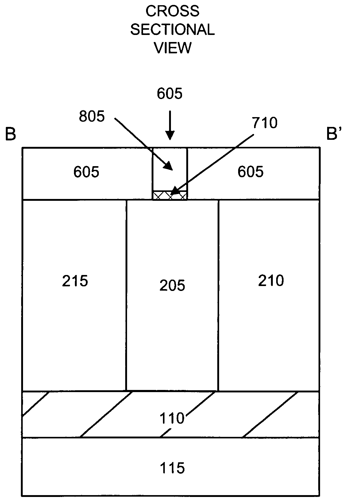
[0026]The following detailed description of the invention refers to the accompanying drawings. The same reference numbers in different drawings may identify the same or similar elements. Also, the following detailed description does not limit the invention. Instead, the scope of the invention is defined by the appended claims.
[0027]Consistent with the present invention, an exemplary damascene process for forming a FinFET that minimizes buried oxide undercutting is provided. In the exemplary damascene process, a sacrificial oxide layer is formed over the FinFET fin such that subsequent etching to form the FinFET gate does not undercut the buried oxide layer upon which the fin has been formed. After formation of the sacrificial oxide layer, a dummy gate may be formed from a layer of semiconducting material, such as, for example, polysilicon, over the sacrificial oxide layer and the fin. A dielectric layer may then be formed over the FinFET fin, source and drain regions around the dumm...
PUM
 Abstract
Description
Claims
Application Information