Method for patterning a buried oxide thickness for a separation by implanted oxygen (simox) process

a technology of buried oxide and separation process, which is applied in the direction of semiconductor devices, electrical equipment, basic electric elements, etc., can solve the problems of high defect density, disadvantageous technique, and damage to the implanted oxide layer,

Inactive Publication Date: 2001-10-09
IBM CORP
View PDF3 Cites 75 Cited by
  • Summary
  • Abstract
  • Description
  • Claims
  • Application Information

AI Technical Summary

Problems solved by technology

This allows the implant damage to "self anneal" during the implant.
However, this technique is disadvantageous for several reasons.
For example, there is a high density of defects (e.g., primarily dislocations) formed beneath the mask edge region.
Thus, the number

Method used


Image

  • Method for patterning a buried oxide thickness for a separation by implanted oxygen (simox) process
  • Method for patterning a buried oxide thickness for a separation by implanted oxygen (simox) process
  • Method for patterning a buried oxide thickness for a separation by implanted oxygen (simox) process

Examples


first embodiment

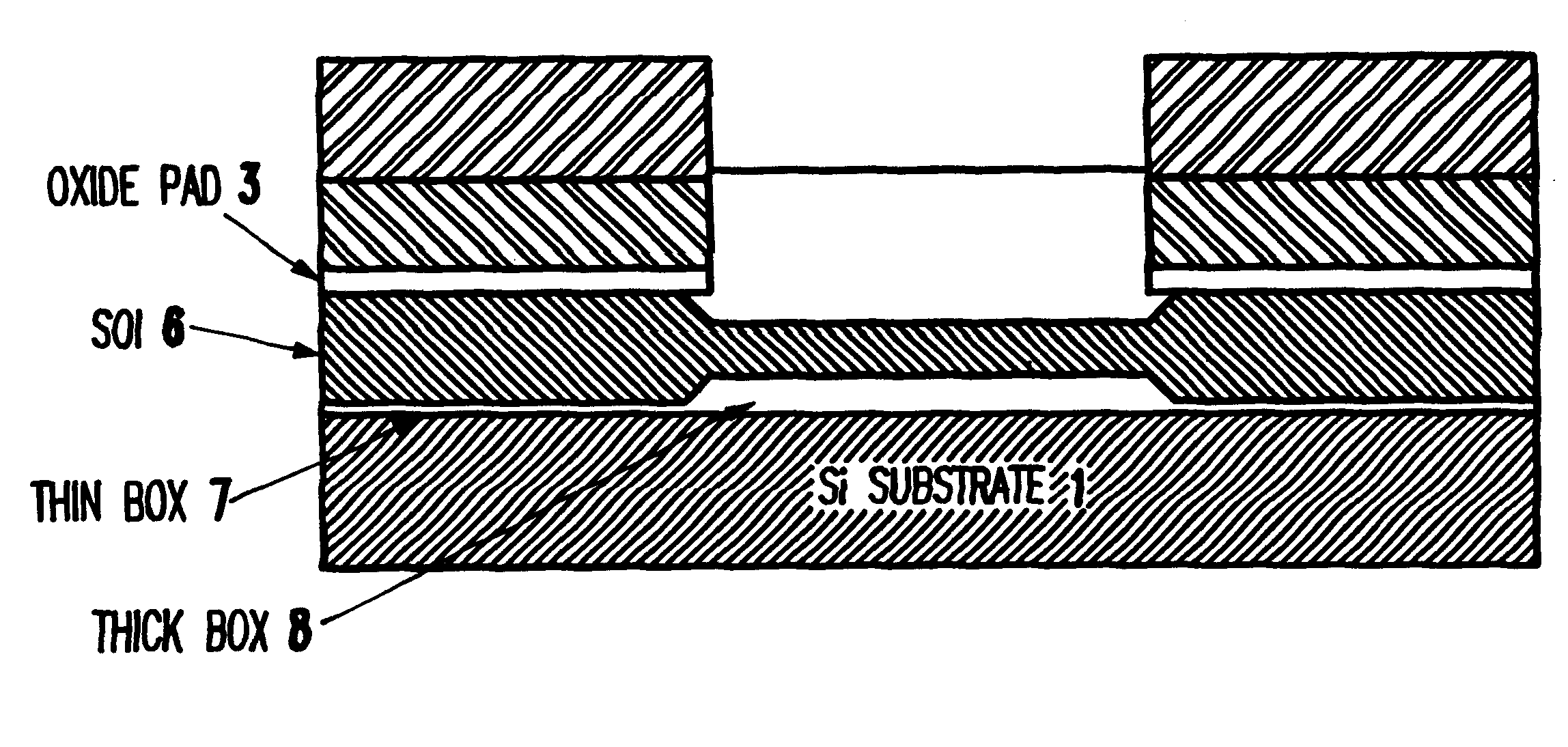
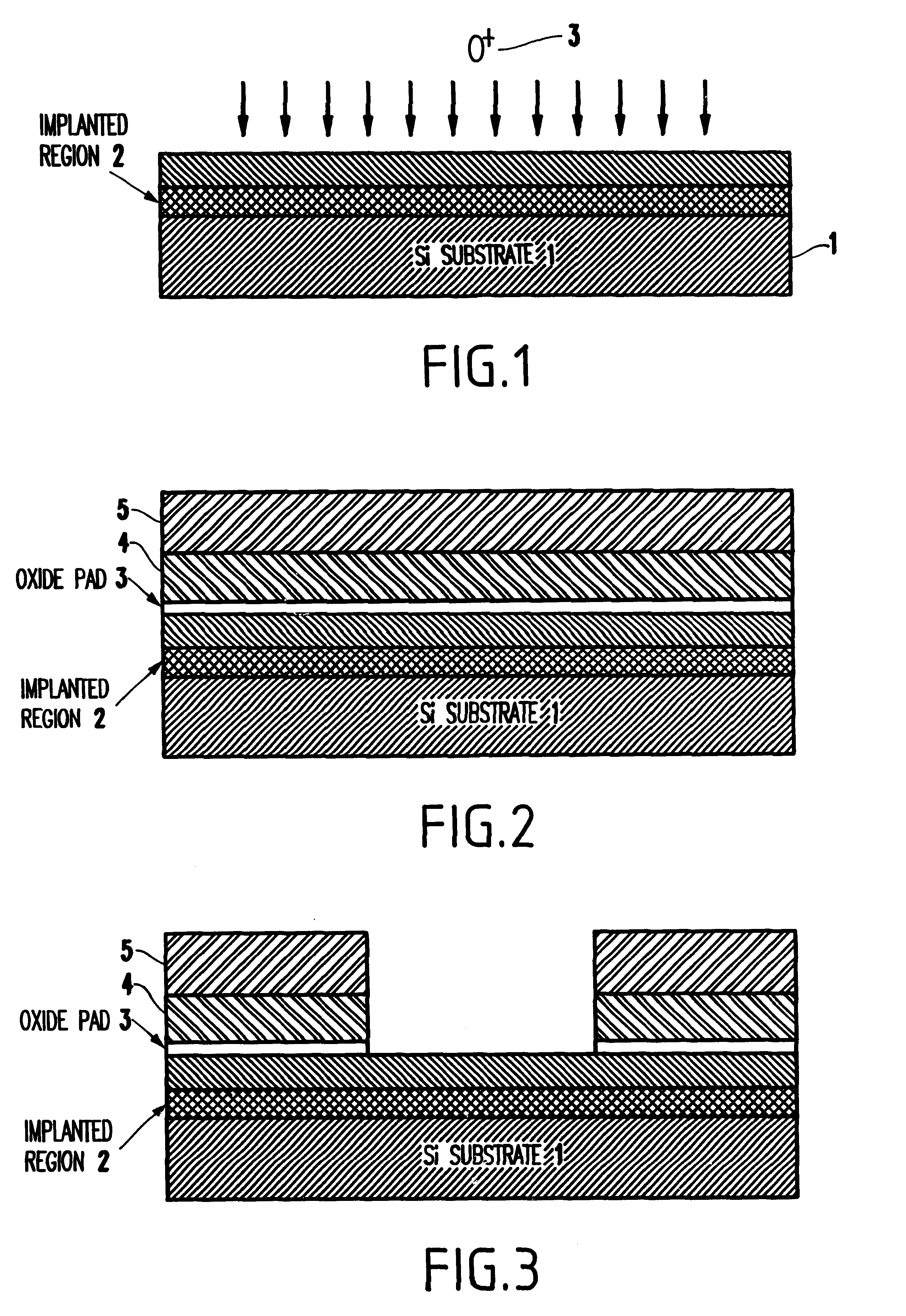
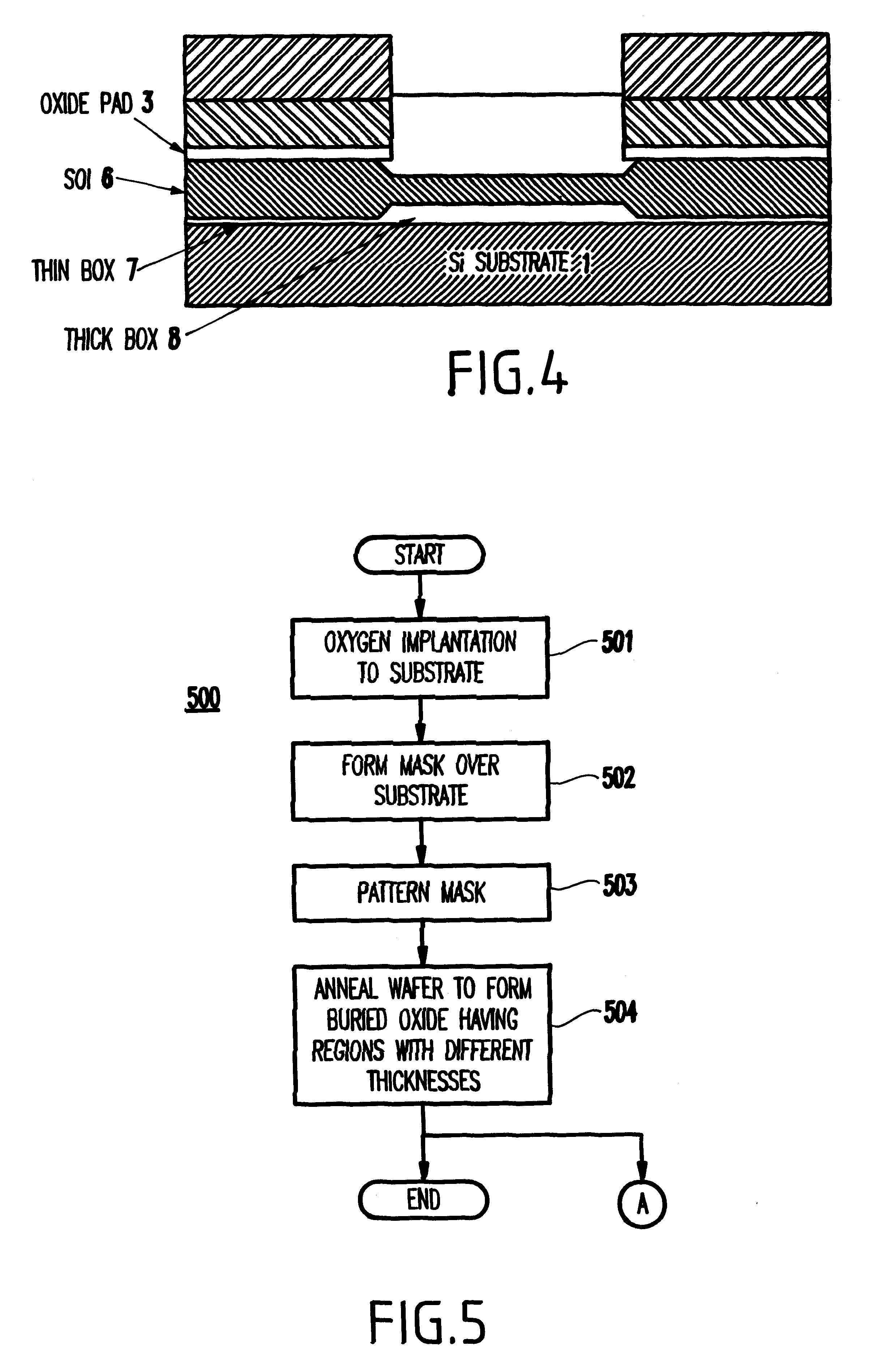
Referring to FIGS. 1-8 and 10, a first embodiment of method for fabricating a patterned buried oxide film according to the present invention will be described below.

Referring to FIG. 1, first an implant 3 (e.g., oxygen, nitrogen to form a buried nitrogen film, or a combination thereof; for illustration purposes, oxygen will be employed as described below) is implanted into a substrate 1 (e.g., formed of silicon, silicon-germanium (SiGe) silicon carbide (SiC), etc.; for illustration purposes, a silicon substrate will be employed as described below) using an energy of about 30 KeV to about 400 KeV, and more preferably 210 KeV, and a wafer temperature of between approximately 600.degree. C. to 650.degree. C. A typical implanted oxygen dose used is in the range of 10.sup.18 cm.sup.-2, or 2.times.10.sup.17 to 4.times.10.sup.17 cm.sup.-2. Other implant energies and oxygen doses may be used depending on the desired SOI and BOX thickness. The implanted region is shown at reference numeral 2...

second embodiment

Referring to FIG. 9, a second embodiment of the invention will be described below.

Specifically, one drawback of the above-described process of the first embodiment is that the top SOI surface is non-planar. In some situations, this may not be desirable. Accordingly, if a planarized surface is desired, a second embodiment of a method 900 of the present invention may be utilized as shown in FIG. 9. It is noted that the second embodiment is performed after the first embodiment has been performed.

That is, in step 901, the anneal mask is stripped (e.g., preferably by a selective etch). For example, the nitride mask may be stripped by hot phosphoric acid (H.sub.3 PO.sub.4), whereas the LTO and pad oxide may be stripped with hydrofluoric acid (DHF 10:1).

Then, in step 902, the silicon is grown epitaxially. This epitaxial growth process will fill all trenches if a sufficiently thick film is grown. Such a thickness depends on the topography that must be planarized. For example, silicon epitax...


PUM


Abstract

A method of forming a patterned buried oxide film, includes performing an implantation into a substrate, forming a mask on at least portions of the substrate for controlling the implantation diffusion, and annealing the substrate to form a buried oxide. The mask may be selectively patterned. A region that is covered by the mask has a thinner buried oxide than an area which is exposed directly to the annealing ambient.

Description

1. Field of the InventionThe present invention relates to a novel technique for the fabrication of a semiconductor device, and more particularly to a method for producing a patterned buried oxide (BOX) film for a semiconductor device.2. Description of the Related ArtComplementary Metal Oxide Semiconductor (CMOS) circuits, which are fabricated using Silicon On Insulator (SOI) wafers have important advantages over conventional bulk CMOS, such as the absence of latch-up, a reduced parasitic drain-source capacitance, ease of making shallow junctions, and higher immunity to soft-errors (e.g., see J. P. Colinge, Silicon-On-Insulator Technology: materials to VLSI, 2.sup.nd Ed., Kluwer Academic Publishers, 1997).The use of SOI wafers is not limited to CMOS. Micro-machining applications also use SOI wafers for the fabrication of sensors and thermally isolated detectors. Separation by Implanted Oxygen (SIMOX) is currently the main technique used for the fabrication of Silicon-On-Insulator (SO...

Claims


Application Information

Patent Timeline
IPC IPC(8): H01L21/70H01L21/762H01L21/76H01L21/02H01L21/265H01L27/12
CPCH01L21/76243H01L21/31
Inventor COHEN, GUY MOSHESADANA, DEVENDRA KUMAR
Owner IBM CORP
Why Eureka
Try Eureka