Method for Forming Dielectric Film Containing Si-C bonds by Atomic Layer Deposition Using Precursor Containing Si-C-Si bond

a technology of atomic layer deposition and dielectric film, which is applied in the direction of coating, chemical vapor deposition coating, metallic material coating process, etc., can solve the problem of narrow controllable ranges using process parameters, the burden of handling halogen-containing materials, and the inability to provide good step covering properties. good and other problems, to achieve the effect of excellent step coverag

Inactive Publication Date: 2013-08-29
ASM IP HLDG BV
View PDF31 Cites 428 Cited by
  • Summary
  • Abstract
  • Description
  • Claims
  • Application Information

AI Technical Summary

Benefits of technology

[0013]A reactant gas constituted by predominantly a rare gas in an excited state can reach sidewall and bottom surfaces of fine patterns of a substrate and effectively reacts with a precursor having a Si—C—Si bond chemisorbed on the surfaces, thereby forming a film having an excellent step coverage in a manner less dependent on pattern density. Preferably, He is used as a reactant gas in an oxygen-free and halogen-free environment.

Problems solved by technology

However, as finer patterning is required, it becomes more difficult for the conventional method to provide not only good step covering property but also pattern density independency.
However, handling halogen-containing materials exerts additional burdens on operation systems, and controllable ranges using process parameters are narrow since the processes still require both film formation and etching to obtain desired dimensions of films conforming to the shapes and dimensions of an underlying layer on which the films are deposited.

Method used


Image

  • Method for Forming Dielectric Film Containing Si-C bonds by Atomic Layer Deposition Using Precursor Containing Si-C-Si bond
  • Method for Forming Dielectric Film Containing Si-C bonds by Atomic Layer Deposition Using Precursor Containing Si-C-Si bond
  • Method for Forming Dielectric Film Containing Si-C bonds by Atomic Layer Deposition Using Precursor Containing Si-C-Si bond

Examples


example

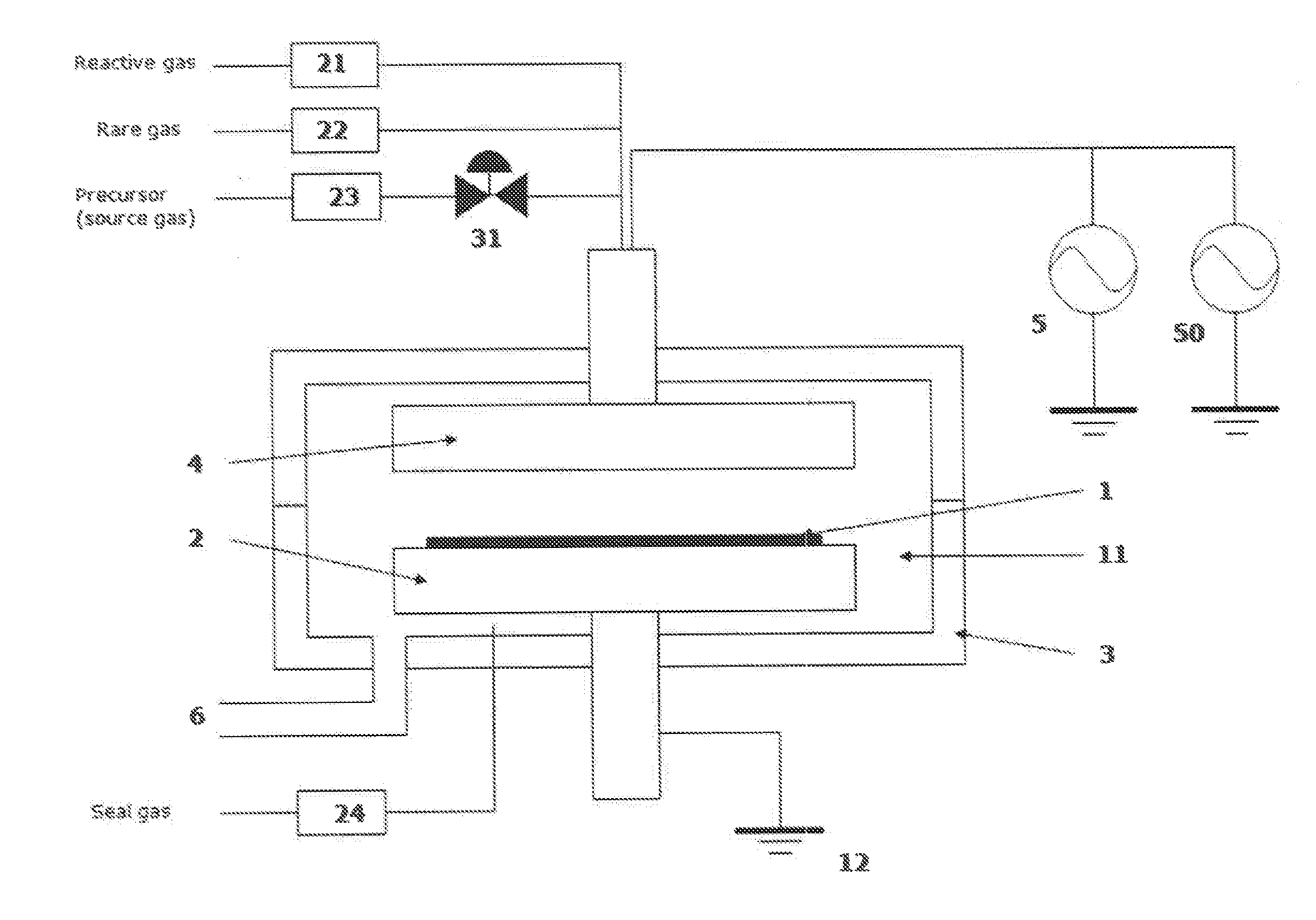
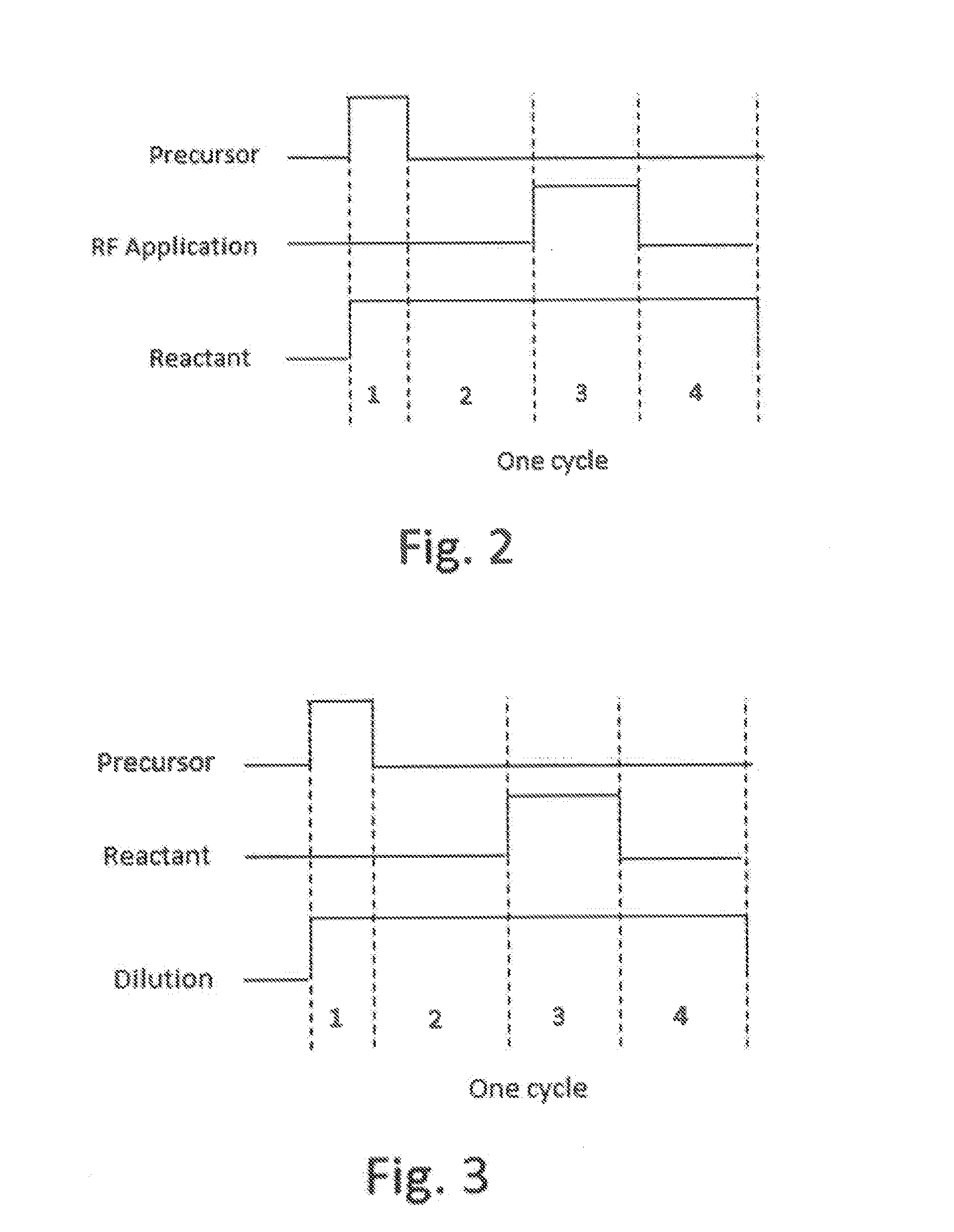
[0081]Conventionally, for forming a silicon oxide film by ALD, aminosilane materials are often used, and thus, formation of SiCN and SiC films using an amonosilane precursor was evaluated. As a reactant, H2, CH4, N2, NH3, and He were used. All of the reactants successfully reacted with the adsorbed aminosilane precursor; however, when film was formed on semiconductor circuits having recesses, the thickness of film deposited on a sidewall was smaller than that of film deposited on a bottom surface or a top surface. This problem is caused by insufficient plasma reaction by reactant species with the adsorbed precursor at the sidewall and bottom surface. For a blanket film formed on a flat horizontal surface, the growth rate per cycle was confirmed to change along a saturation curve in relation to gas supply time and purge time.

[0082]In ALD, reactivity between an adsorbed precursor and a reactant is uniquely dependent upon what type of precursor and what type of reactant are used in com...


PUM

PropertyMeasurementUnit
pressureaaaaaaaaaa
pressureaaaaaaaaaa
thicknessaaaaaaaaaa

Abstract

A method of forming a dielectric film having Si—C bonds on a semiconductor substrate by atomic layer deposition (ALD), includes: (i) adsorbing a precursor on a surface of a substrate; (ii) reacting the adsorbed precursor and a reactant gas on the surface; and (iii) repeating steps (i) and (ii) to form a dielectric film having at least Si—C bonds on the substrate. The precursor has a Si—C—Si bond in its molecule, and the reactant gas is oxygen-free and halogen-free and is constituted by at least a rare gas.

Description

BACKGROUND OF THE INVENTION[0001]1. Field of the Invention[0002]The present invention relates generally to semiconductor integrated circuit manufacturing and, more particularly to a method of forming a dielectric film having at least Si—C bonds on a semiconductor substrate by atomic layer deposition (ALD).[0003]2. Description of the Related Art[0004]SiC, SiCN, SiN and other silicon-containing insulation films were adopted as etching stopper films and Cu diffusion blocking films for devices installed with Cu wiring. For installing devices with Cu wiring, damascene structures are widely used, and as a result, these films are effectively adapted as etching stopper films and Cu diffusion blocking films by modifying their characteristics depending on required specifications. When applying these films to damascene structures, since films are formed mostly on planar surfaces, those skilled in the art have been forming these films using plasma CVD, where the films tend to possess low dielec...

Claims


Application Information

Patent Timeline
Patent Type & Authority Applications(United States)
IPC IPC(8): H01L21/31
CPCH01L21/02167H01L21/02274H01L21/0228C23C16/56C23C16/4554C23C16/5096C23C16/325
Inventor FUKAZAWA, ATSUKITAKAMURE, NOBORU
Owner ASM IP HLDG BV
Why Eureka
Try Eureka