Double-sided integrated circuit chips

Active Publication Date: 2007-11-22
GLOBALFOUNDRIES US INC
View PDF22 Cites 86 Cited by
  • Summary
  • Abstract
  • Description
  • Claims
  • Application Information

AI Technical Summary

Benefits of technology

[0011]A ninth aspect of the present invention is a the first aspect, wherein the first devices are N-channel field effect transistors, sources and drains thereof are in tension and the second devices are P-channel field effect transistors sources and drains thereof are in compression.
[0012]A tenth aspect of the present

Problems solved by technology

This can be difficult and costly to accomplish when; for example, thermal cycles that are required by one set of devices can adversely affect other devices on the same int

Method used


Image

  • Double-sided integrated circuit chips
  • Double-sided integrated circuit chips
  • Double-sided integrated circuit chips

Examples


Embodiment Construction

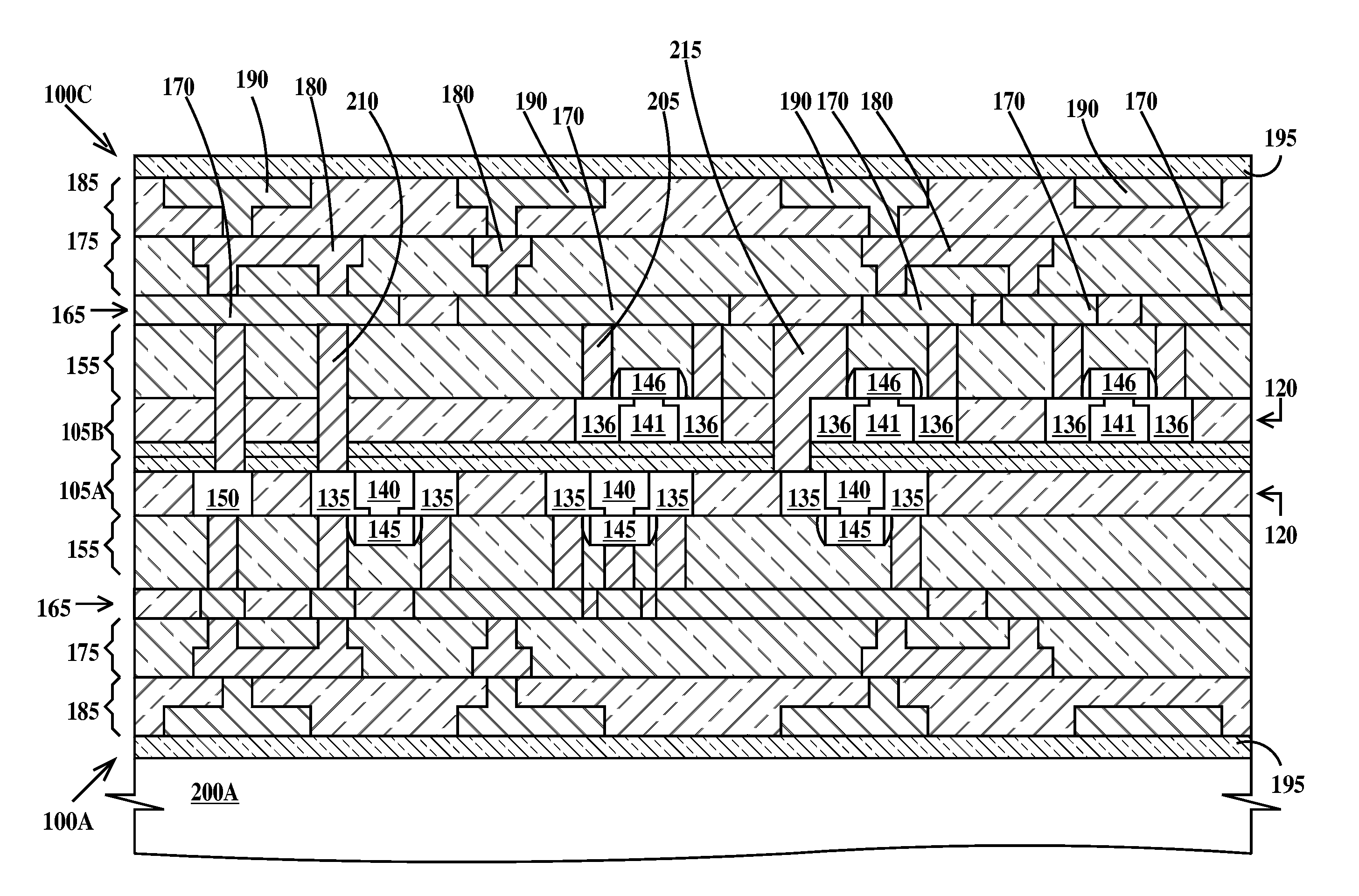
[0023]It should be understood that the integrated circuit chips of the embodiments of the present invention are advantageously formed on integrated circuit substrates called wafers and that multiple integrated circuits may be fabricated simultaneously on the same wafer and may be separated by a dicing process after fabrication is complete.

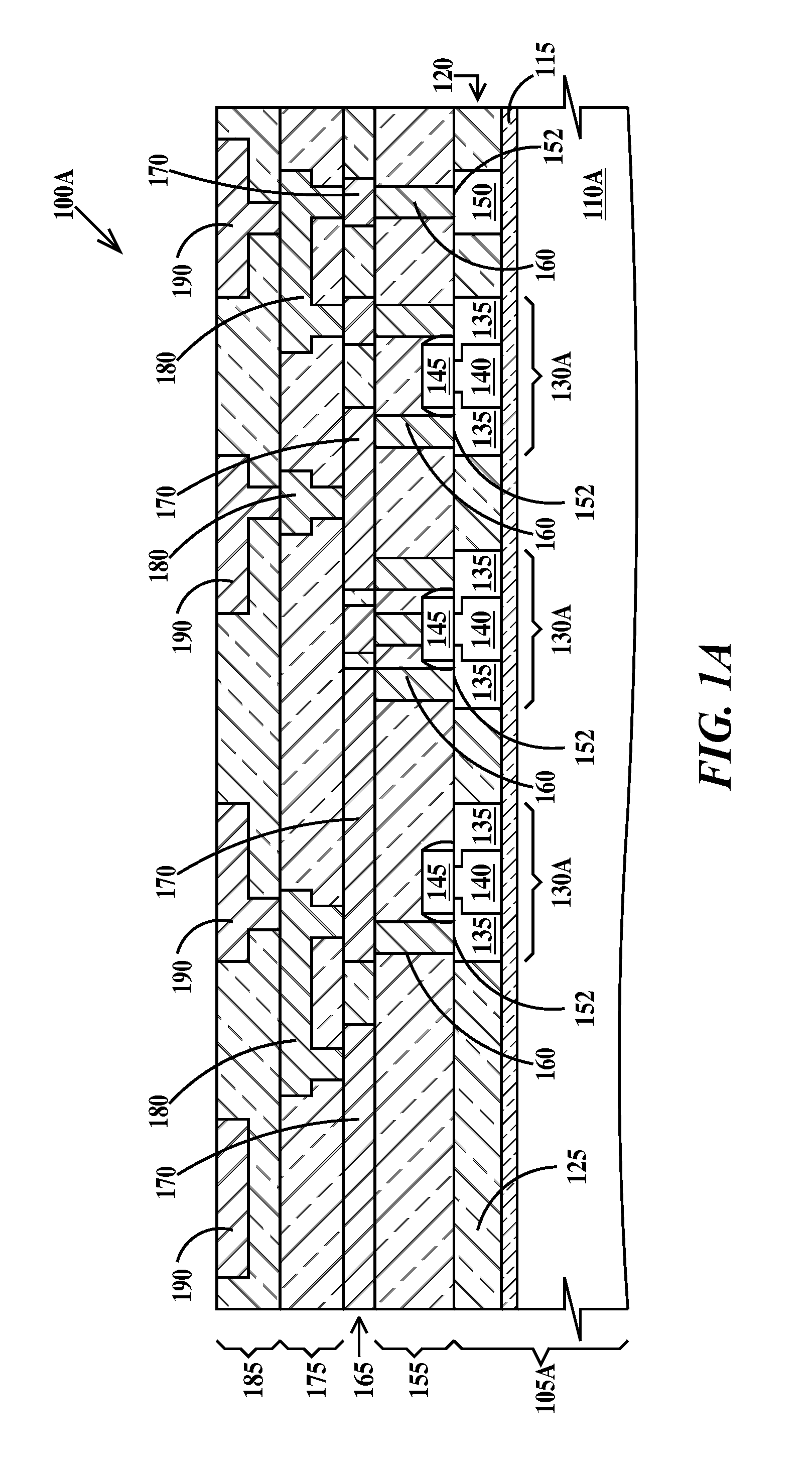
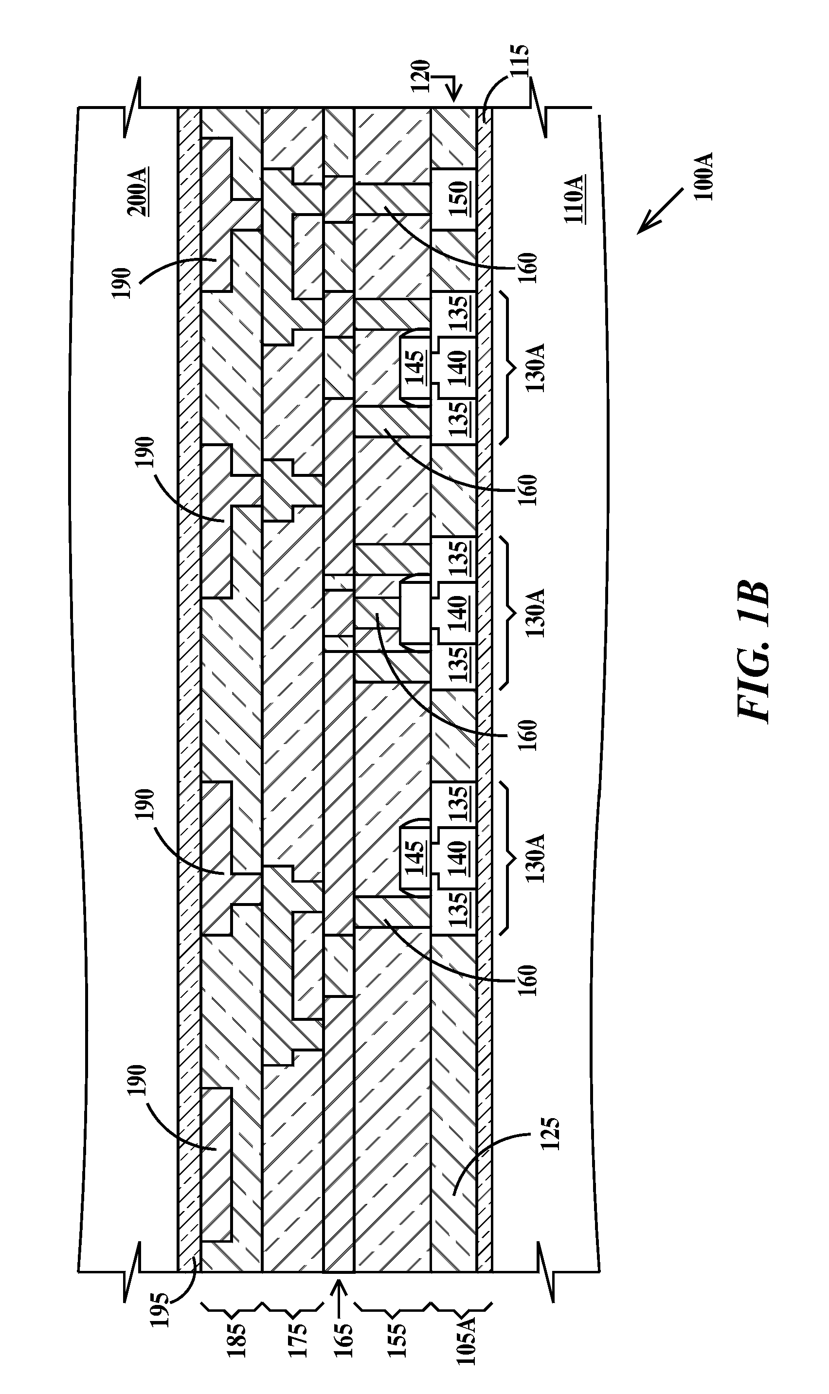
[0024]FIGS. 1A through 1J are cross-sectional drawings illustrating fabrication of an integrated circuit chip according to a first embodiment of the present invention. In FIG. 1A, a first wafer 100A is fabricated through pad level. Wafer 100A includes a silicon-on-insulator (SOI) substrate 105A which includes a silicon substrate 110A, a buried oxide layer (BOX) 115 formed on the silicon substrate and a single-crystal silicon layer 120 formed on the BOX. Formed in silicon layer 120 is trench isolation 125 and source / drains 135 and channel regions 140 of field effect transistors (FETs) 130A. Also formed in silicon layer 120 are optional silicon regio...


PUM


Abstract

A semiconductor structure and method of fabricating the structure. The method includes removing the backside silicon from two silicon-on-insulator wafers having devices fabricated therein and bonding them back to back utilizing the buried oxide layers. Contacts are then formed in the upper wafer to devices in the lower wafer and wiring levels are formed on the upper wafer. The lower wafer may include wiring levels. The lower wafer may include landing pads for the contacts. Contacts to the silicon layer of the lower wafer may be silicided.

Description

FIELD OF THE INVENTION[0001]The present invention relates to the field of integrated circuits; more specifically, it relates to double-sided integrated circuit chips and methods of fabricating double sided integrated circuit chips.BACKGROUND OF THE INVENTION[0002]To maximize the performance of integrated circuits the fabrication process is adjusted to enhance the performance of different devices and circuits in different regions of the integrated circuit chip. This can be difficult and costly to accomplish when; for example, thermal cycles that are required by one set of devices can adversely affect other devices on the same integrated circuit chip. Further, it is often difficult to center the fabrication process tightly around the device specifications for different types of device simultaneously. Therefore, there is a need for integrated circuit chips and methods of fabricating integrated circuit chips wherein the fabrication process may be adjusted to enhance the performance of d...

Claims


Application Information

Patent Timeline
IPC IPC(8): H01L23/52H01L21/44
CPCH01L23/481H01L23/522H01L23/5329H01L25/0657H01L25/50H01L27/0688H01L2924/0002H01L2225/06513H01L2225/06527H01L2924/00H01L21/76895
Inventor BERNSTEIN, KERRYDALTON, TIMOTHY JOSEPHGAMBINO, JEFFREY PETERJAFFE, MARK DAVIDKARTSCHOKE, PAUL DAVIDLUCE, STEPHEN ELLINWOODSTAMPER, ANTHONY KENDALL
Owner GLOBALFOUNDRIES US INC
Why Eureka
Try Eureka