Method of producing soi wafer and soi wafer

a technology of soi wafer and soi wafer, which is applied in the direction of basic electric elements, electrical apparatus, and semiconductor devices, can solve the problems of void generation, disadvantage in cost, and uniform thickness of soi layer achieved by ion implantation/delamination, and achieve good crystallinity, good crystallinity, and high yield

Inactive Publication Date: 2005-06-02
SHIN-ETSU HANDOTAI CO LTD
View PDF14 Cites 73 Cited by
  • Summary
  • Abstract
  • Description
  • Claims
  • Application Information

AI Technical Summary

Benefits of technology

[0027] If an SOI wafer is produced by the above method of producing an SOI wafer of the present invention, there can be provided an SOI wafer without generating blisters and voids even when the thickness of its buried oxide film is thin, and its SOI layer has extremely good crystallinity.
[

Problems solved by technology

However, when producing an SOI wafer, if the mirror polishing process including an element of machining has been carried out at the final stage as described above, there occurs a problem that uniformity of the thickness of the SOI layer achieved by the ion implantation/delamination is degraded because the polishing stock removal is not uniform.
Moreover, since the mirror polishi

Method used


Image

  • Method of producing soi wafer and soi wafer
  • Method of producing soi wafer and soi wafer
  • Method of producing soi wafer and soi wafer

Examples


example 1

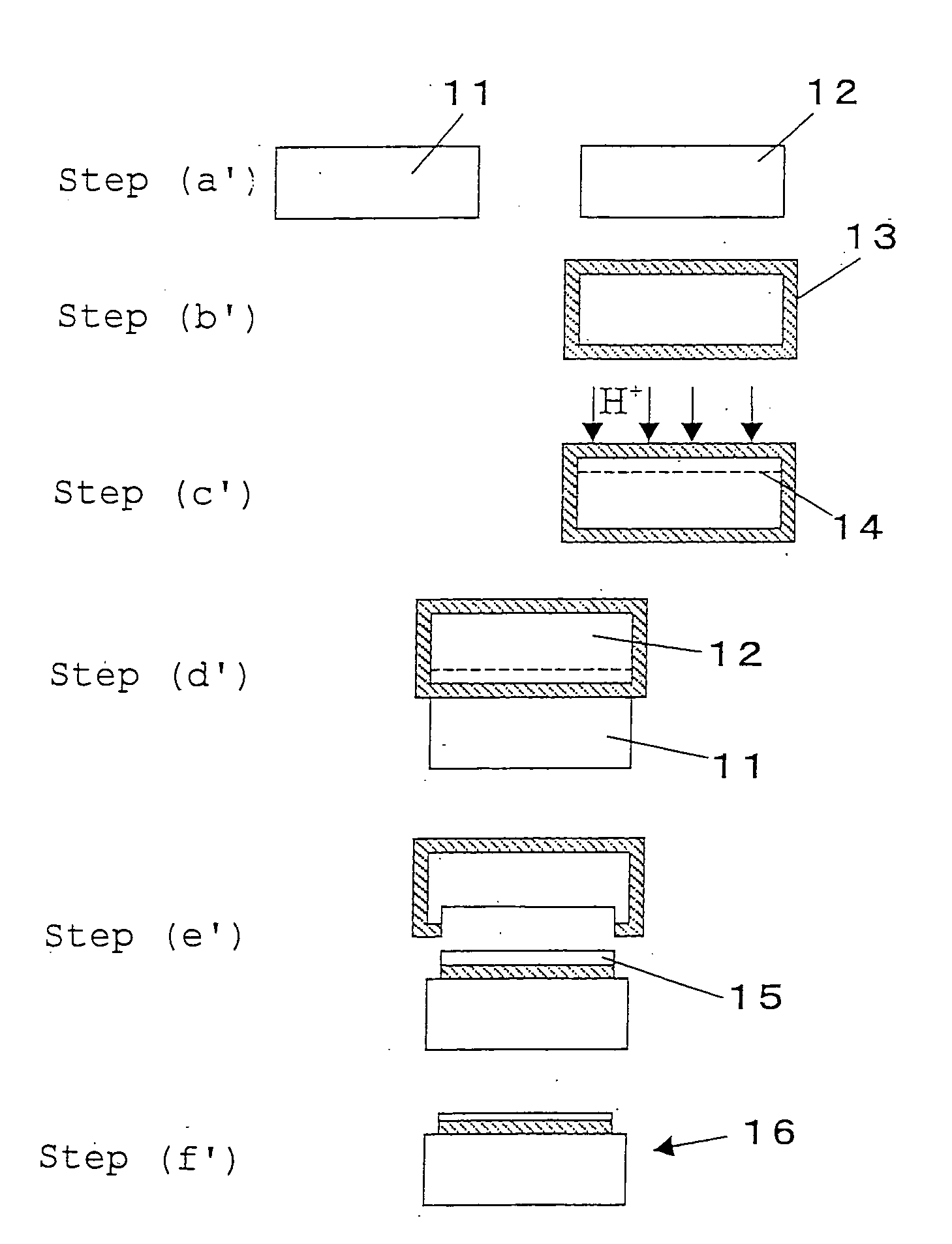
[0057] Mirror-polished silicon wafers having a diameter of 200 mm were prepared to produce an SOI wafer having a buried oxide film with a thickness of 80 nm as a product standard by an ion implantation delamination method.

[0058] First, after a silicon wafer to be a bond wafer was thermally oxidized to form an oxide film having a thickness of 100 nm on a surface of the silicon wafer, hydrogen ions were implanted into the silicon wafer at implantation energy of 53 keV (Implantation dose: 5.5×10¹⁶ / cm2) to form an ion-implanted layer. Then, after the bond wafer was bonded to a base wafer through the oxide film, delaminating heat treatment was performed in a nitrogen atmosphere at 500° C. for 30 minutes to delaminate the bond wafer at the ion-implanted layer, a wafer having an SOI layer was produced. The obtained bonded wafer was subjected to a touch polishing with a stock removal of 60 nm to form the SOI layer having a thickness of 320 nm.

[0059] After that, the bonded wafer was subjec...

example 2

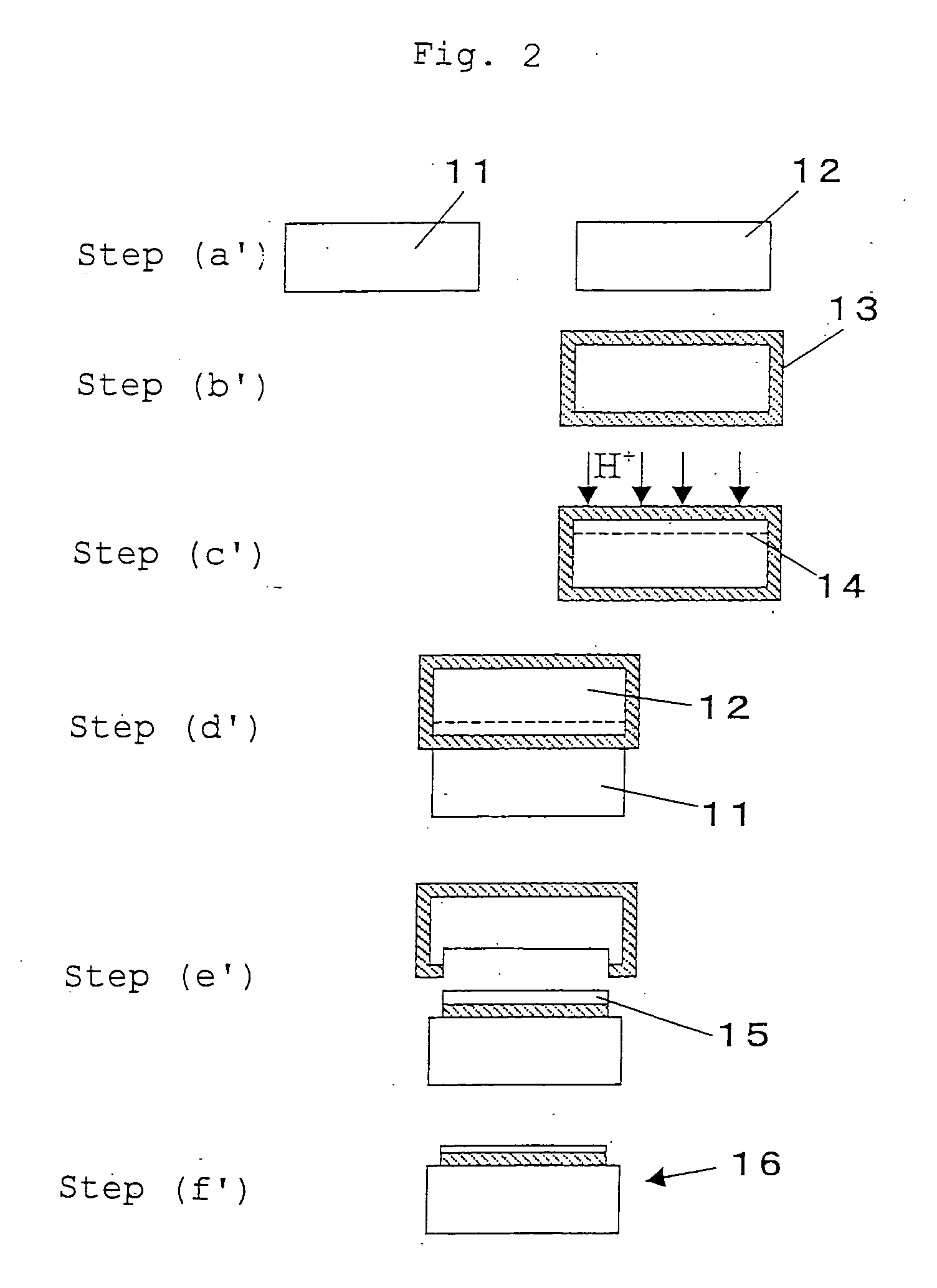
[0060] Mirror-polished silicon wafers having a diameter of 200 mm were prepared to produce an SOI wafer having a buried oxide film with a thickness of 30 nm as a product standard by an ion implantation delamination method.

[0061] First, after a bond wafer was thermally oxidized to form an oxide film having a thickness of 80 nm on a surface of the silicon wafer, hydrogen ions were implanted into the silicon wafer at implantation energy of 50 keV (Implantation dose: 5.5×10¹⁶ / cm2) to form an ion-implanted layer. Then, after the bond wafer was bonded to a base wafer having an oxide film with a thickness of 20 nm on its surface through the oxide film, delaminating heat treatment was performed in a nitrogen atmosphere at 500° C. for 30 minutes to delaminate the bond wafer at the ion-implanted layer, a wafer having an SOI layer was produced. The obtained bonded wafer was subjected to a touch polishing with a stock removal of 60 nm to form the SOI layer having a thickness of 320 nm.

[0062] ...


PUM


Abstract

The present invention relates to a method of producing an SOI wafer in which an SOI layer is formed on a buried oxide film by forming an oxide film on a surface of at least one of a bond wafer and a base wafer, bonding the bond wafer to the base wafer through the formed oxide film, and making the bond wafer into a thin film, wherein after the oxide film is formed so that a total thickness of the oxide film formed on the surface of at least one of the bond wafer and the base wafer is thicker than a thickness of the buried oxide film that the SOI wafer to be produced has, the bond wafer is bonded to the base wafer through the formed oxide film, the bond wafer is made into a thin film to form an SOI layer, and thereafter, an obtained bonded wafer is subjected to heat treatment to reduce a thickness of the buried oxide film. Thereby, there can be provided a method of producing an SOI wafer in which blisters and voids are not generated even if the thickness of the buried oxide film is thinned, and its SOI layer has extremely good crystallinity.

Description

TECHNICAL FIELD [0001] The present invention relates to a method of producing an SOI (Silicon On Insulator) wafer having SOI structure in which a silicon layer is formed on an insulator, and an SOI wafer produced by the method thereof. BACKGROUND ART [0002] Recently, an SOI wafer having SOI structure in which a silicon layer (an SOI layer) is formed on an insulator has been especially attracting attention as a wafer for high-performance LSI for an electronic device because the SOI wafer is excellent in high-speed property, low power consumption, high breakdown voltage, environmental resistance, etc. of the device. [0003] Representative production methods of the SOI wafer are SIMOX method in which an oxide film is formed in a silicon wafer by subjecting to heat treatment at a high temperature after implanting oxygen ions into the silicon wafer at high concentration, a method called a bonding method, etc. The bonding method is a method of producing an SOI wafer in which an SOI layer i...

Claims


Application Information

Patent Timeline
IPC IPC(8): H01L21/02H01L21/265H01L21/762H01L27/12
CPCH01L21/76254H01L21/26533
Inventor AGA, HIROJIYOKOKAWA, ISAOTAKANO, KIYOTAKAMITANI, KIYOSHI
Owner SHIN-ETSU HANDOTAI CO LTD
Why Eureka
Try Eureka