Extremely-thin silicon-on-insulator transistor with raised source/drain

Active Publication Date: 2009-02-12
GLOBALFOUNDRIES US INC +1
View PDF10 Cites 87 Cited by
  • Summary
  • Abstract
  • Description
  • Claims
  • Application Information

AI Technical Summary

Benefits of technology

[0007]Briefly, in accordance with the present invention, disclosed are a method, transistor, and integrated circuit. According to one embodiment, there is provided an ETSOI transistor that includes a buried oxide layer above a substrate, a silicon layer above the buried oxide layer, a gate stack on the silicon layer, a nitride liner having a first part on the silicon layer and a second part adjacent to the gate stack, an oxide liner having a first part on the first part of the nitride liner and a second

Problems solved by technology

However, an ETSOI transistor with a high-K dielectric and gate stack without proper spacers suffers from the growth of an underlayer of oxide that lowers the gate capacitance.
However, the formation of a raised source/drain also requires the use of spacers for selective epitaxial growth, which leads to silicon loss during reactive-ion etching (“RIE”) of the spacer.
This underlayer of oxide (or “underoxide”) lowers the gate capacitance, which is not desirable.
The oxide spacer is in contact with the high-K gate oxide, which leads

Method used


Image

  • Extremely-thin silicon-on-insulator transistor with raised source/drain
  • Extremely-thin silicon-on-insulator transistor with raised source/drain
  • Extremely-thin silicon-on-insulator transistor with raised source/drain

Examples


Embodiment Construction

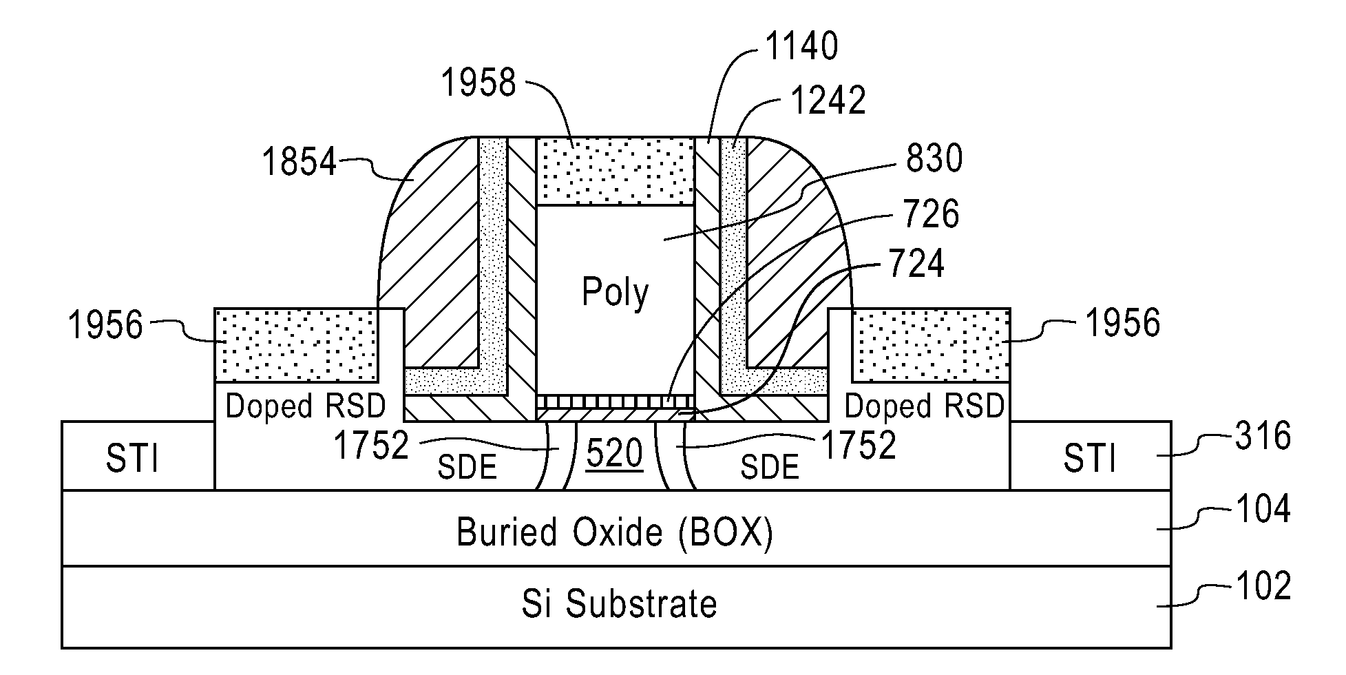
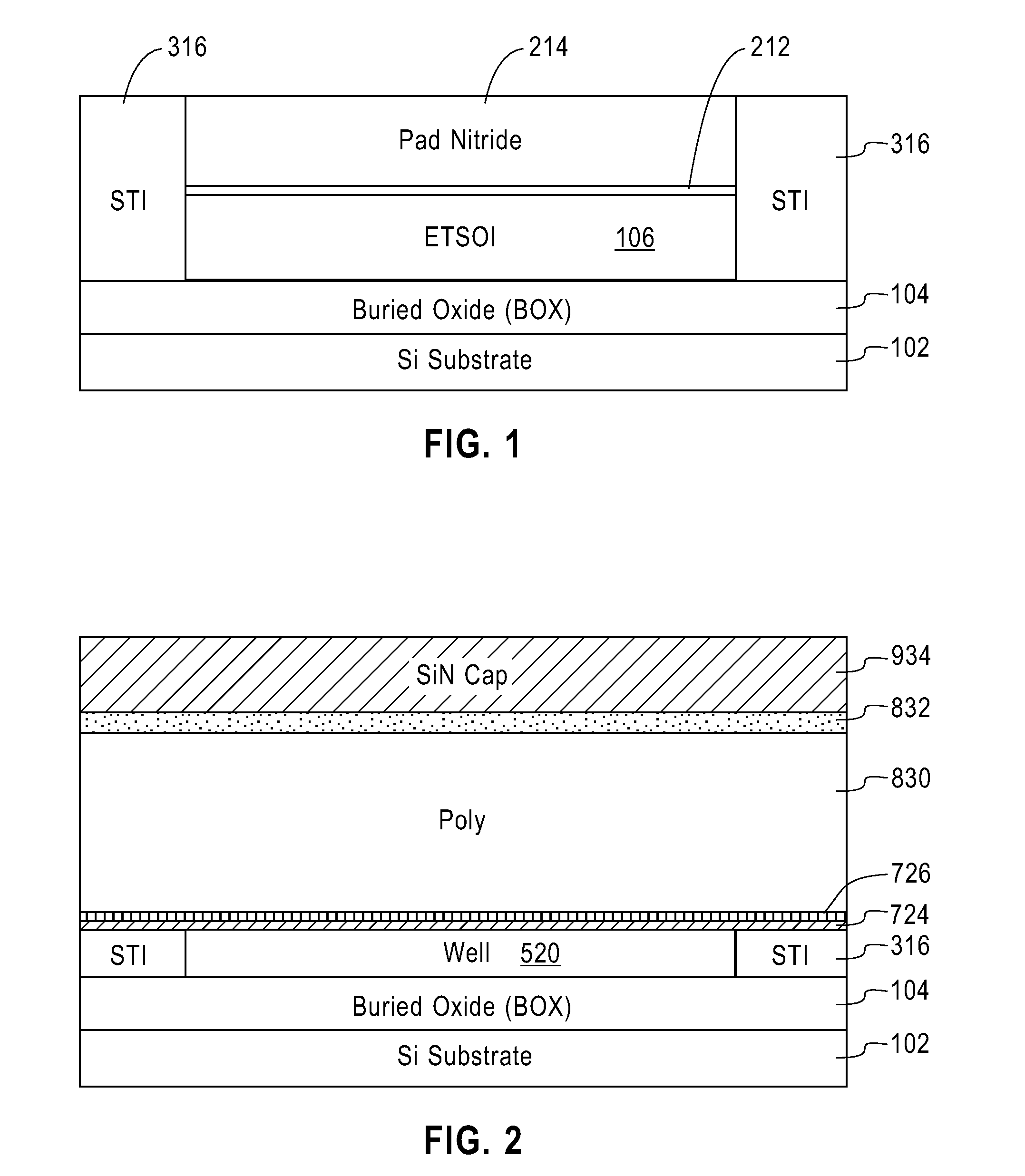
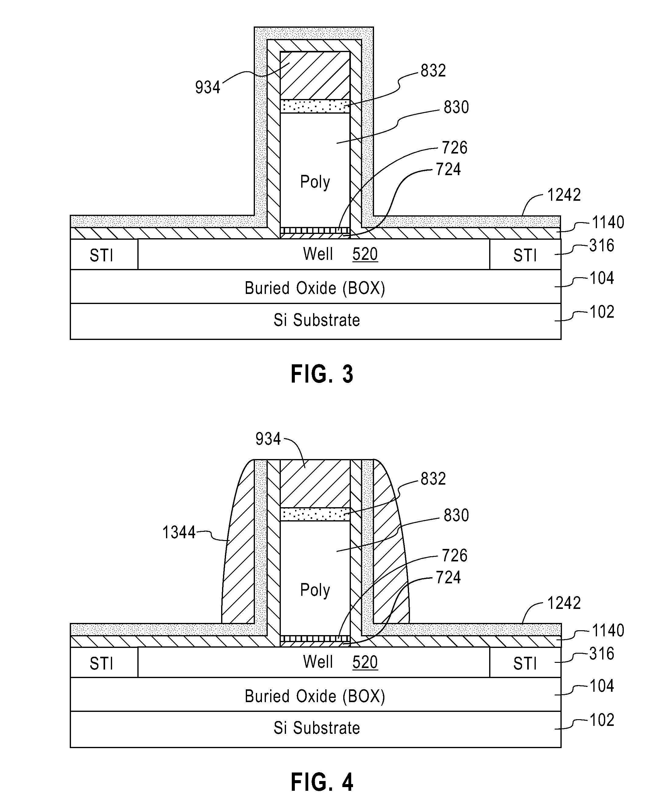
[0012]Embodiments of the present invention provide extremely-thin silicon-on-insulator (“ETSOI”) field-effect transistors with a thin spacer structure of nitride and oxide layers. This spacer structure enables the transistors to be formed with a high-K dielectric and metal gate stack and a raised source / drain, without underoxide growth beneath the high-K dielectric and without silicon loss during spacer formation.

[0013]FIGS. 1 to 9 illustrate a process for forming an extremely-thin silicon-on-insulator transistor according to an embodiment of the present invention. The process begins with an SOI wafer that is formed by a silicon substrate 102, a buried oxide layer (“BOX”) 104, and an ETSOI layer 106. In this embodiment, the SOI wafer is a “thin” SOI wafer having a thickness in the 15-30 nm range. Alternatively, the process can begin with a “thick” SOI wafer having a thickness in the 30-90 nm range, and thinning can be performed using oxidation and a hydrofluoric acid (HF) wet etch t...


PUM


Abstract

An extremely-thin silicon-on-insulator transistor is provided that includes a buried oxide layer above a substrate, a silicon layer above the buried oxide layer, a gate stack on the silicon layer, a nitride liner on the silicon layer and adjacent to the gate stack, an oxide liner on and adjacent to the nitride liner, and raised source/drain regions. The gate stack includes a high-k oxide layer on the silicon layer and a metal gate on the high-k oxide layer. Each of the raised source/drain regions has a first part comprising a portion of the silicon layer, a second part adjacent to parts of the oxide liner and the nitride liner, and a third part above the second part. Also provided is a method for fabricating an extremely-thin silicon-on-insulator transistor.

Description

FIELD OF THE INVENTION[0001]The present invention generally relates to the field of semiconductors, and more particularly relates to extremely-thin silicon-on-insulator field-effect transistors with a raised source / drain structure and a method for fabricating the same.BACKGROUND OF THE INVENTION[0002]Complementary Metal Oxide Semiconductor (“CMOS”) Field Effect Transistors (“FETs”) are employed in almost every electronic circuit application, such as signal processing, computing, and wireless communications. One known type of FET is a Silicon-On-Insulator (“SOI”) FET. An SOI transistor with a very thin SOI body thickness and optional light halo doping has very good short channel control. More information of such SOI transistors is available in the references B. Doris et al., “Extreme scaling with ultra-thin Si channel MOSFETs” (IEDM Technical Digest, 2002); B. Doris et al., “Device design considerations for ultra-thin SOI MOSFETs” (IEDM Technical Digest, 2003); and D. V. Singh et al....

Claims


Application Information

Patent Timeline
IPC IPC(8): H01L29/786H01L21/336
CPCH01L21/28079H01L29/4958H01L29/665H01L29/6653H01L29/78696H01L29/6656H01L29/6659H01L29/66628H01L29/66772H01L29/66537
Inventor CARTIER, EDUARD A.KOESTER, STEVEN J.MAITRA, KINGSUKMAJUMDAR, AMLANMO, RENEE T.
Owner GLOBALFOUNDRIES US INC
Why Eureka
Try Eureka