Process and lead frame for making leadless semiconductor packages

a leadless semiconductor and lead frame technology, applied in semiconductor devices, semiconductor/solid-state device details, electrical apparatus, etc., can solve the problems of reducing the market competitiveness of leadless packages. achieve the effect of convenient implementation

Active Publication Date: 2006-08-08
ADVANCED SEMICON ENG INC
View PDF9 Cites 70 Cited by
  • Summary
  • Abstract
  • Description
  • Claims
  • Application Information

AI Technical Summary

Benefits of technology

[0011]Thereafter, each lead of the lead frame is electrically coupled to two different bonding pads of one of the chips such that the first portion of each lead is electrically connected to one bonding pad and the second portion of each lead is electrically connected to the other bonding pad. After a tape is attached onto the lower surface of the lead frame, the chips are encapsulated against the upper surface of the lead frame to form a molded product. After the tape is removed from the bottom of the molded product, a second metal layer is selectively plated on the first portions and the second portions of the leads and the die pads exposed from the bottom of the molded product wherein the second metal layer is not provided on the second portions of the leads. Then, the third portion of each lead of the lead frame is selectively etched away such that the first portion and the second portion are electrically isolated from each other and become two connection pads. Finally, a singulation step is conducted to obtain the leadless semiconductor packages. Note that each lead of the lead frame is selectively etched away the third portion thereof thereby forming two rows of connection pads. In this way, the number of I / O connections is significantly increased while the pitch or spacing between adjacent leads is not required to be reduced. Accordingly, the finished leadless semiconductor packages satisfy the need for a significantly higher number of connection pads in a smaller footprint.
[0014]According to another aspect of the invention, there is provided another lead frame designed to make the staggered multi-row leadless packages. This lead frame includes first and second leads arranged about the periphery of the die pad in each unit. Each of the first leads has one end connected to the dambars. Each of the second leads has an enlarged portion adapted for electrically coupling to the semiconductor chip and a narrowed portion connected to the dambars. Such kind of lead frame design is fully compatible with the existing materials and does not affect their properties; it is cheap and of extremely easy implementation. In addition, the packaging method using the aforementioned lead frame is fully compatible with the current processes and related equipment used in the industry.

Problems solved by technology

However, as integrated circuits products move its endless pace toward both a faster speed and a smaller size, the traditional lead frame packages have become gradually obsolete for some high performance-required packages.
Traditional lead frame package has its limit of providing a solution for chip scale and low profile package due to the long inner leads and outer leads.
However, the conventional leadless package 10 has various design and production limitations.
Such an increase in the density of leads inherently requires a reduced pitch or spacing between adjacent leads thereby increasing likelihood of cross-talk and signal interference and making such packages more difficult to fabricate.

Method used


Image

  • Process and lead frame for making leadless semiconductor packages
  • Process and lead frame for making leadless semiconductor packages
  • Process and lead frame for making leadless semiconductor packages

Examples


Embodiment Construction

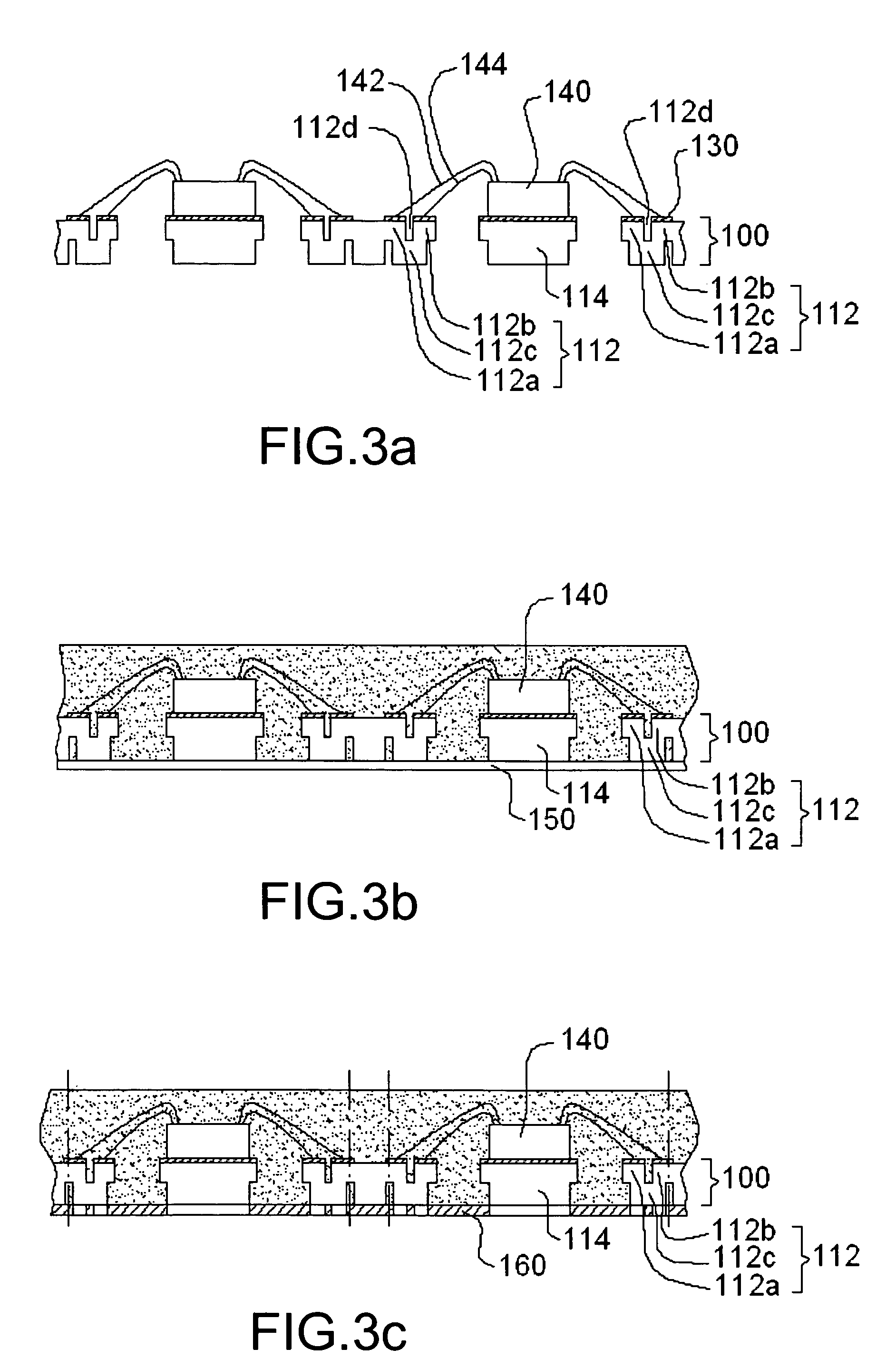
[0022]FIGS. 3a to 3g illustrate in cross-section major steps of a process for making a plurality of staggered dual-row leadless packages using the lead frame 100 shown in FIG. 4 according to one embodiment of the present invention.

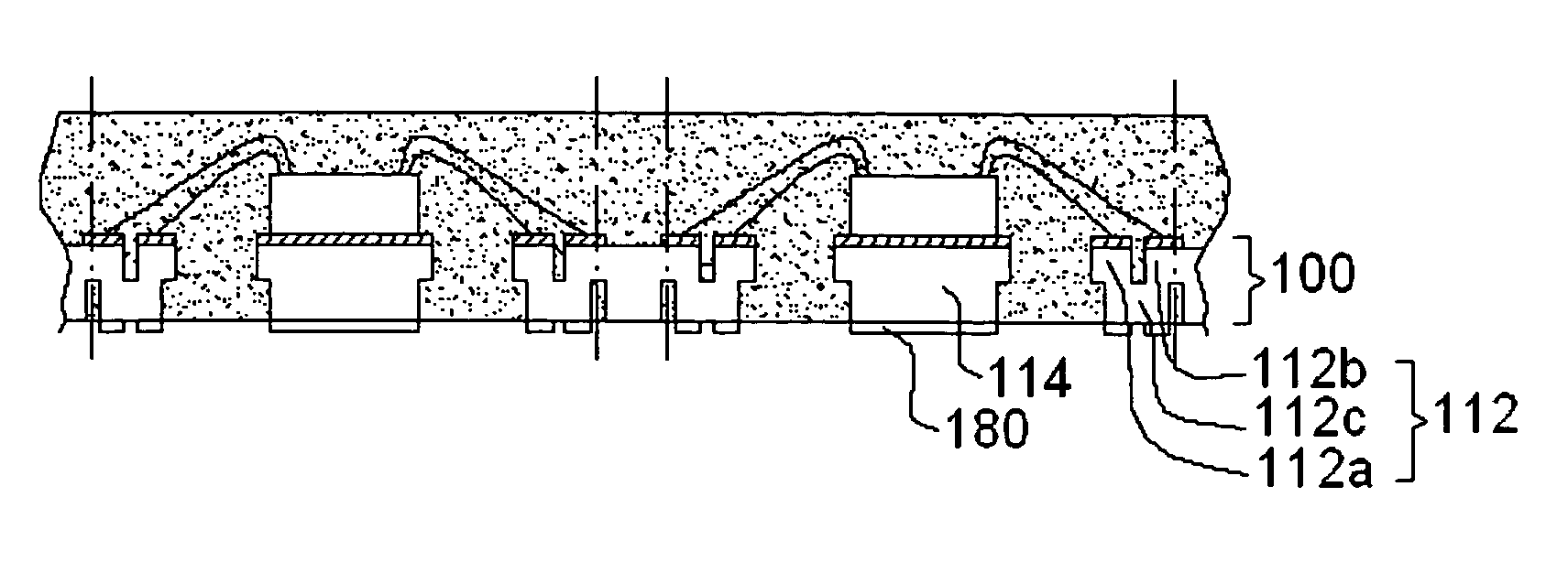
[0023]As shown in FIG. 4, the lead frame 100 includes a plurality of units 110 in an array arrangement. The units 110 of the lead frame 100 are separated from each other by a plurality of dambars 120 which generally form an orthogonal grid on the lead frame 100. Though only four units 110 are shown in FIG. 4, a lead frame for use with the invention can include any number of units if desired. Each of the units 110 of the lead frame includes a plurality of leads 112 (only one lead is denoted with the numeral 112 in FIG. 4 for simplicity) arranged at the periphery of a die pad 114. Each die pad 11b is connected to the dambars 120 by four tie bars 116 (only one tie bar is denoted with the numeral 116 in FIG. 4 for simplicity). Each of the leads 112 has a first...


PUM


Abstract

A process for making a plurality of leadless packages is disclosed. Firstly, chips are attached onto a lead frame with a first metal layer formed thereon. Each lead of the lead frame has a first portion, a second portion and a third portion connecting the first portion and the second portion, wherein the first metal layer is not provided on the third portion. After a wire bonding step and an encapsulating step are conducted, a second metal layer is selectively plated on the first portions and the second portions of the leads and the die pads exposed from the bottom of the molded product. Then, the third portion of each lead is selectively etched away such that the first portion and the second portion are electrically isolated from each other. Finally, a singulation step is conducted to complete the process. The present invention further provides a new lead frame design.

Description

BACKGROUND OF THE INVENTION[0001]1. Field of the Invention[0002]This invention relates to a process and a lead frame for making leadless semiconductor packages.[0003]2. Description of the Related Art[0004]Lead frame packages have been used for a long period of time in the IC packaging history mainly because of their low manufacturing cost and high reliability. However, as integrated circuits products move its endless pace toward both a faster speed and a smaller size, the traditional lead frame packages have become gradually obsolete for some high performance-required packages. Thus BGA (Ball Grid Array Packages) and CSP (Chip Scale Package) have emerged and become increasingly popular as a new packaging choice.[0005]However, the lead frame package still remains its market share as a cost-effective solution for low I / O ICs. Traditional lead frame package has its limit of providing a solution for chip scale and low profile package due to the long inner leads and outer leads. Therefor...

Claims


Application Information

Patent Timeline
Patent Type & Authority Patents(United States)
IPC IPC(8): H01L21/44H01L21/48H01L21/50
CPCH01L21/561H01L23/3107H01L23/49548H01L24/97H01L21/568H01L24/48H01L2224/32245H01L2224/48091H01L2224/48247H01L2224/73265H01L2224/97H01L2924/01029H01L2924/01046H01L2924/01047H01L2924/01078H01L2924/01079H01L2924/01082H01L2924/14H01L2924/30105H01L2924/01033H01L2924/01006H01L2924/01005H01L2224/85H01L2924/00014H01L2224/83H01L2924/00012H01L2924/00H01L24/73H01L2924/181H01L2224/45139H01L2224/45144H01L2224/45147H01L24/45H01L2924/18301H01L2224/45015H01L2924/207
Inventor PARK, HYUNGJUNKIM, HYEONGNOPARK, SANGBAELEE, YONGGILRHO, KYUNGSOOYANG, JUNYOUNGWON, JINHEE
Owner ADVANCED SEMICON ENG INC
Why Eureka
Try Eureka