Methods of forming light-emitting devices having an antireflective layer that has a graded index of refraction

Active Publication Date: 2006-08-08
CREELED INC
View PDF35 Cites 74 Cited by
  • Summary
  • Abstract
  • Description
  • Claims
  • Application Information

AI Technical Summary

Benefits of technology

[0010]Advantageously, by using the antireflective layer to transition between a first medium, e.g., the substrate, and a second medium, e.g., the encapsulation material or air

Problems solved by technology

Unfortunately, the majority of light that is generated inside of an LED device typically never escapes the device because of various optical losses, such as total internal reflection (TIR).
Thus, mediums having sig

Method used


Image

  • Methods of forming light-emitting devices having an antireflective layer that has a graded index of refraction
  • Methods of forming light-emitting devices having an antireflective layer that has a graded index of refraction
  • Methods of forming light-emitting devices having an antireflective layer that has a graded index of refraction

Examples


Embodiment Construction

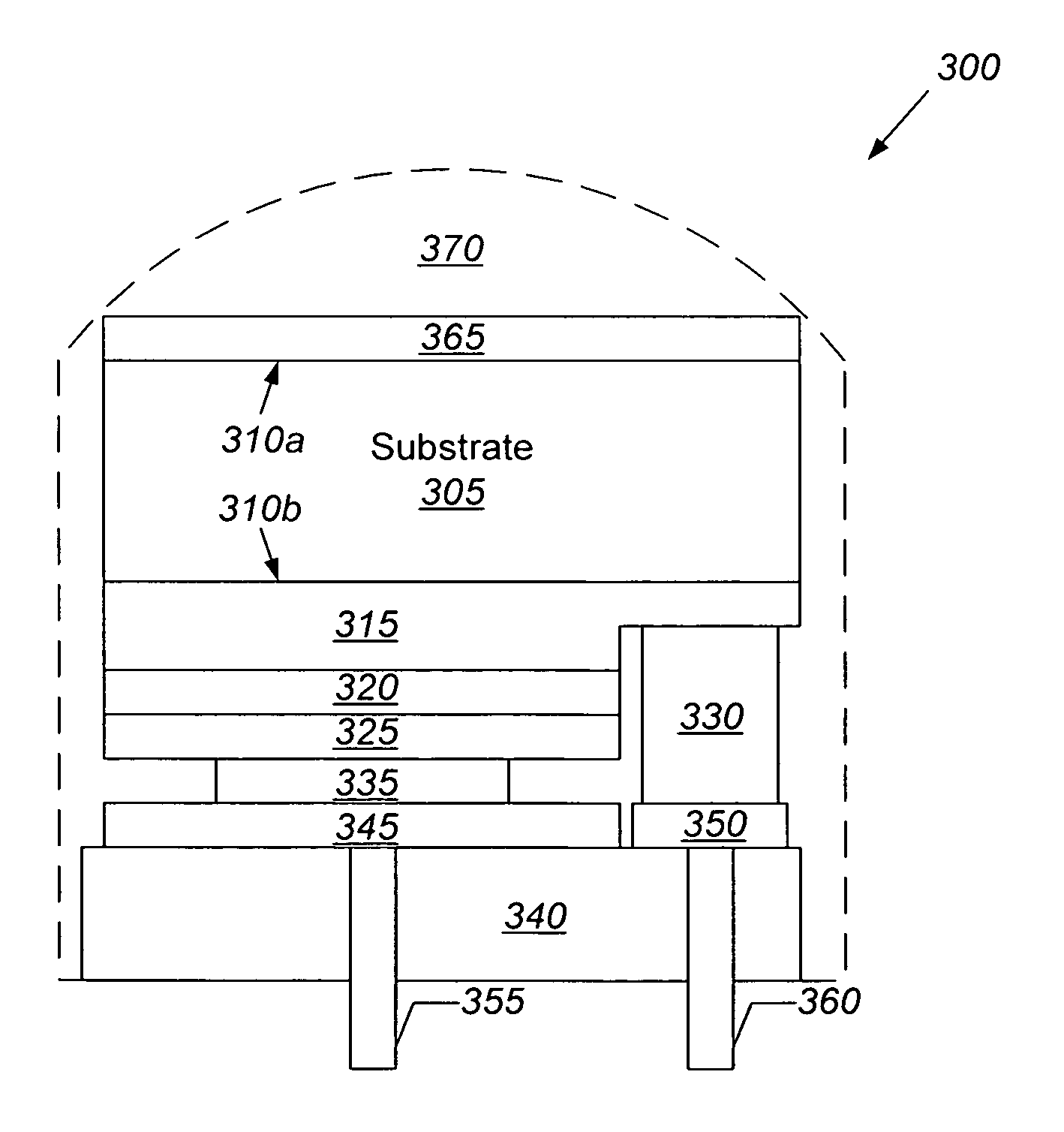
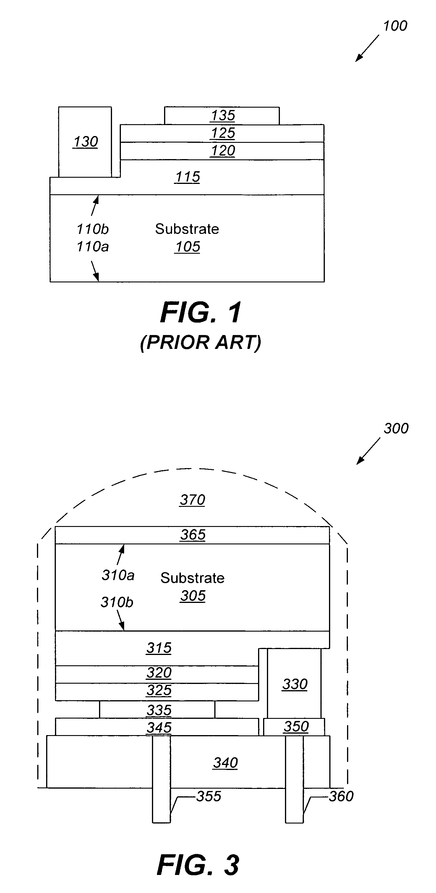
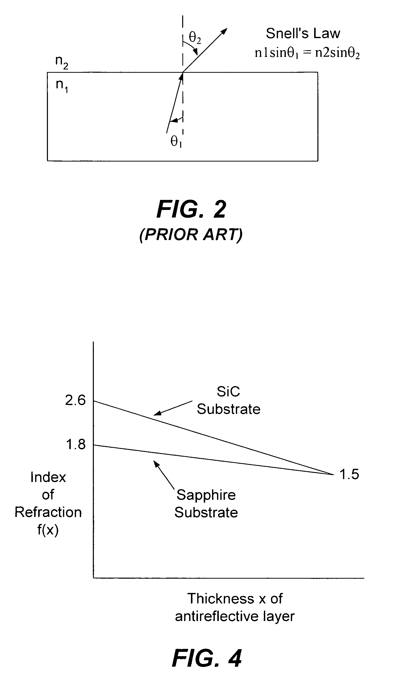
[0024]While the invention is susceptible to various modifications and alternative forms, specific embodiments thereof are shown by way of example in the drawings and will herein be described in detail. It should be understood, however, that there is no intent to limit the invention to the particular forms disclosed, but on the contrary, the invention is to cover all modifications, equivalents, and alternatives falling within the spirit and scope of the invention as defined by the claims. Like numbers refer to like elements throughout the description of the figures. In the figures, the dimensions of layers and regions are exaggerated for clarity. Each embodiment described herein also includes its complementary conductivity type embodiment.

[0025]It will be understood that when an element such as a layer, region or substrate is referred to as being “on” another element, it can be directly on the other element or intervening elements may also be present. It will be understood that if pa...


PUM


Abstract

A light-emitting device includes a substrate that is at least partially transparent to optical radiation and has a first index of refraction. A diode region is disposed on a first surface of the substrate and is configured to emit light responsive to a voltage applied thereto. An encapsulation layer is disposed on a second surface of the substrate and has a second index of refraction. An antireflective layer is disposed between a second surface of the substrate and the encapsulation layer. The antireflective layer has a graded index of refraction having values in a range between about the first index of refraction at a first surface of the antireflective layer and about the second index of refraction at a second surface of the antireflective layer. The encapsulation layer may also be omitted and the antireflective layer may separate the substrate, which has a first index of refraction, from air, which has a second index of refraction. Non “flip-chip” embodiments are also disclosed.

Description

RELATED APPLICATION[0001]This application claims the benefit of and priority to U.S. Provisional Patent Application No. 60 / 466,618, filed Apr. 30, 2003, the disclosure of which is hereby incorporated herein by reference as if set forth in its entirety.BACKGROUND OF THE INVENTION[0002]The present invention relates generally to microelectronic devices and fabrication methods therefor, and, more particularly, to light-emitting devices and fabrication methods therefor.[0003]Light-emitting diodes (LEDs) are widely used in consumer and commercial applications. As is well known to those skilled in the art, a light-emitting diode generally includes a diode region on a microelectronic substrate. The microelectronic substrate may comprise, for example, gallium arsenide, gallium phosphide, alloys thereof, silicon carbide, and / or sapphire. Continued developments in LEDs have resulted in highly efficient and mechanically robust light sources that can cover the visible spectrum and beyond. These ...

Claims


Application Information

Patent Timeline
IPC IPC(8): H01L33/00H01L33/44
CPCH01L33/44
Inventor NEGLEY, GERALD H.
Owner CREELED INC
Why Eureka
Try Eureka