

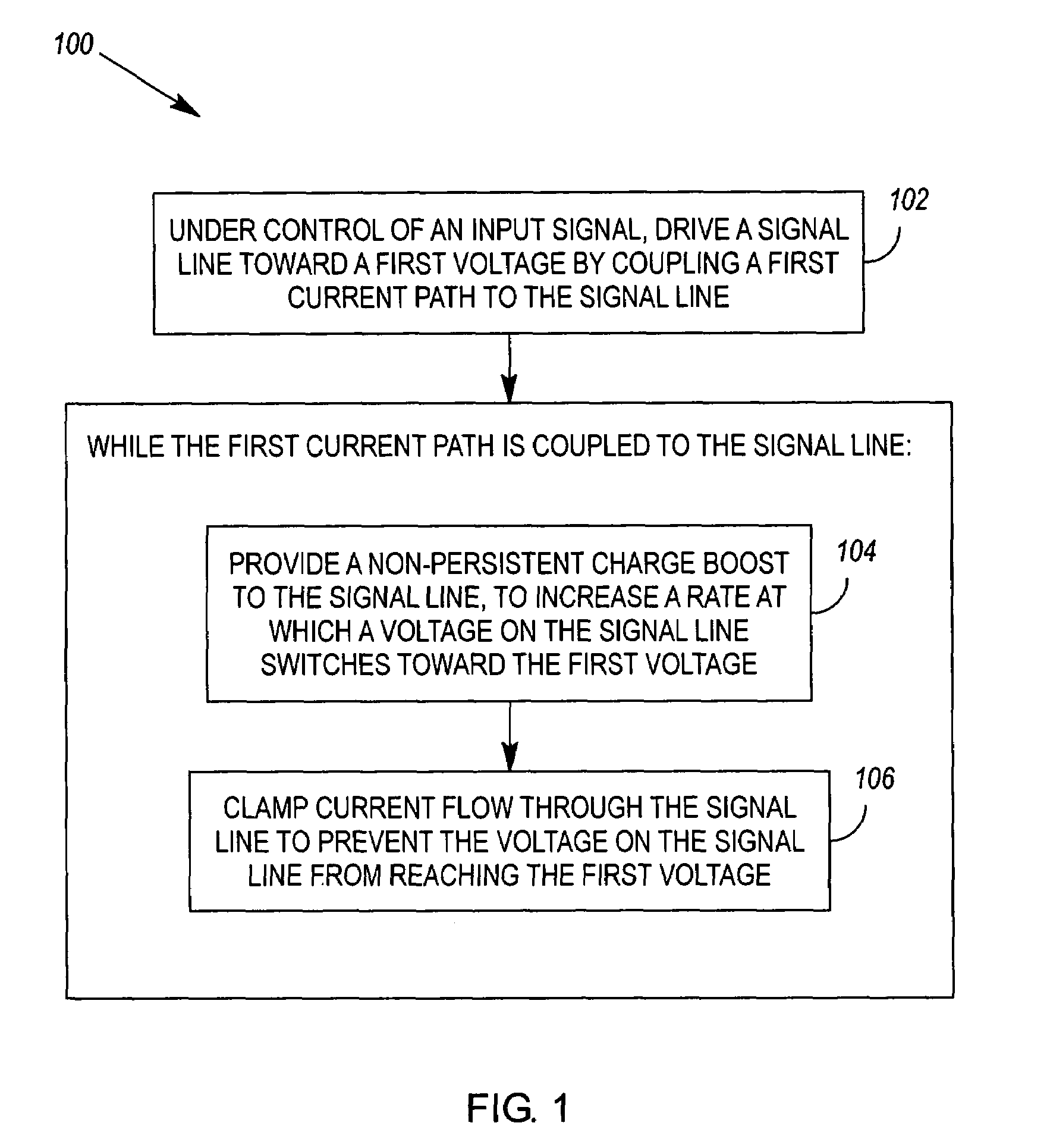
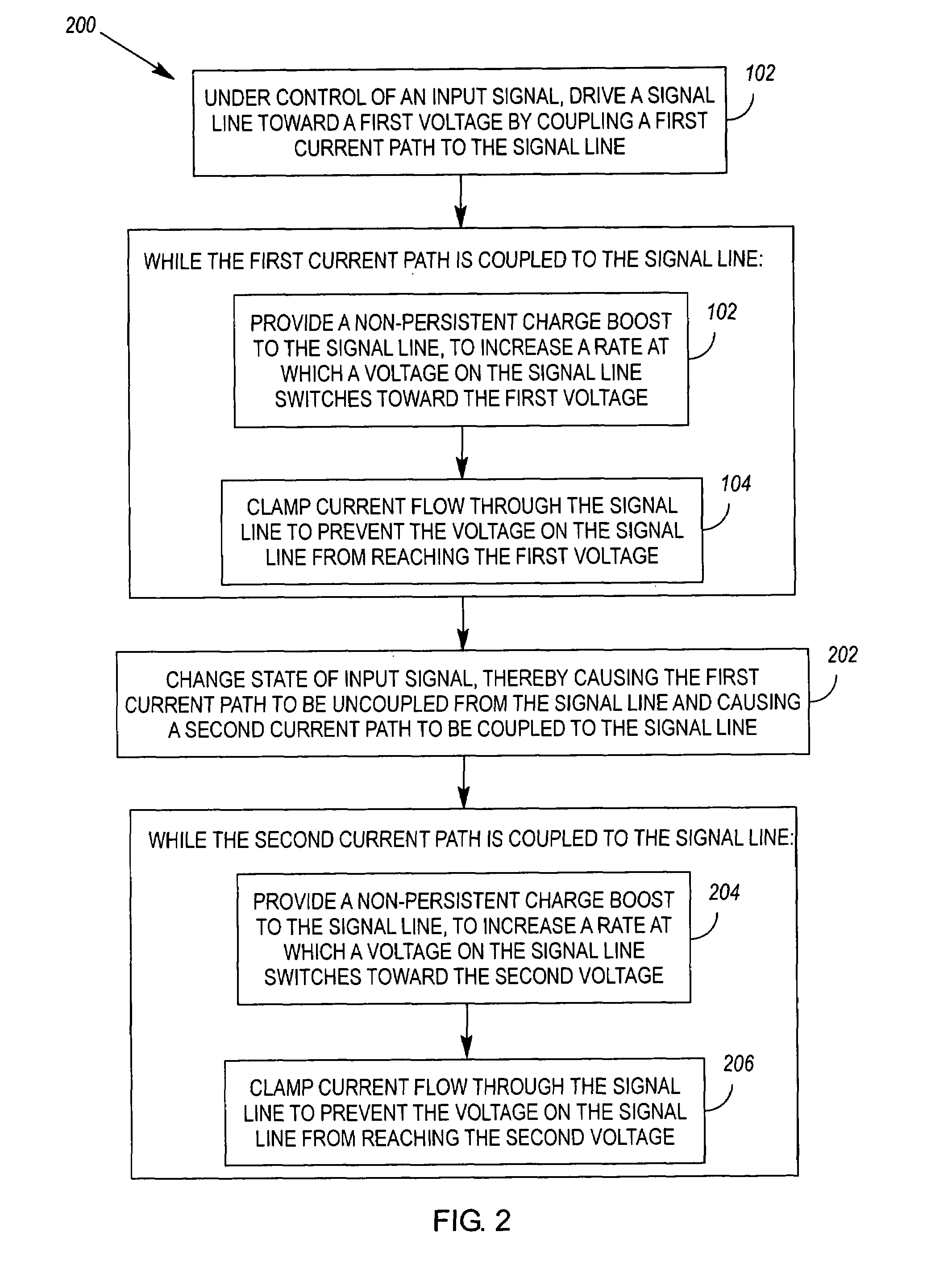
Driver-side current clamping with non-persistent charge boost
a technology of non-persistent charge boost and current clamping, which is applied in the direction of oscillator generators, pulse techniques, logic circuits, etc., can solve the problem that options are typically the most expensive (but sometimes necessary) way to speed signal propagation
- Summary
- Abstract
- Description
- Claims
- Application Information
AI Technical Summary
Benefits of technology
Problems solved by technology
Method used
Image

Examples
first embodiment
[0017]FIG. 3 illustrates a driver circuit 300 that may be used to implement the method 100 or 200. The driver circuit 300 comprises a first current path 302 that is coupled to a first voltage (V1), and a second current path 304 that is coupled to a second voltage (V2). The driver circuit 300 further comprises a first switching means 306 to couple and uncouple the first current path 302 to an output of the driver circuit, and a second switching means 308 to alternately couple and uncouple the second current path 304 to the driver's output. A first current clamping means 310 is coupled in the first current path, and prevents a voltage at the driver output from reaching the first voltage. Likewise, a second current clamping means 312 is coupled in the second current path, and prevents the driver's output voltage from reaching the second voltage. When the first current path 302 is coupled to the driver output, a first non-persistent charge boost means 314, coupled to the first switching...
second embodiment
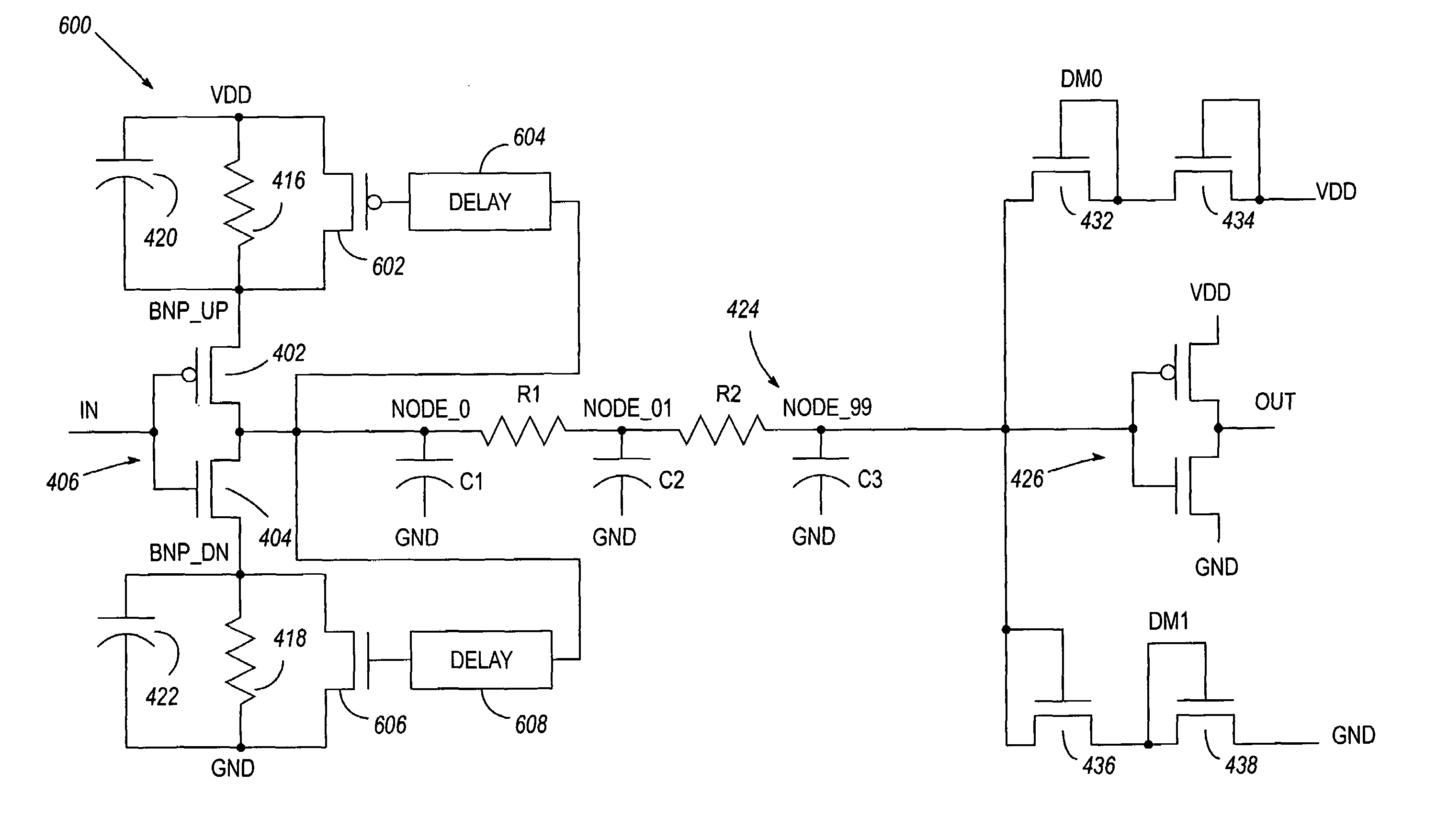
[0019]FIG. 4 illustrates a driver circuit 400 that may be used to implement the method 100 or 200. The driver circuit 400 comprises first and second switching circuits 402, 404, each of which is controlled by an input signal received at node IN. By way of example, the switching circuits 402, 404 may form an inverting complementary metal-oxide semiconductor (CMOS) buffer 406 (i.e., with the first switching circuit taking the form of a p-channel field effect transistor (PFET), and with the second switching circuit taking the form of an n-channel field effect transistor (NFET)). The PFET is coupled via its source and drain between an output of the driver circuit (NODE_0) and a first intermediate node (BNP_UP). The NFET is coupled via its source and drain between NODE_0 and a second intermediate node (BNP_DN). The gates of the two FETs are coupled to each other at node IN, which is configured to receive an input signal.
[0020]The node BNP_UP is coupled to a first voltage (VDD) by means o...
PUM
 Abstract
Description
Claims
Application Information